In this guide, we shall see what is 7 segment display and the difference between Common anode and cathode.
In this guide, we shall cover the following:
- What is 7 segment display.
- Connection of common anode with STM32F4xx.
- Driver.
- Results.
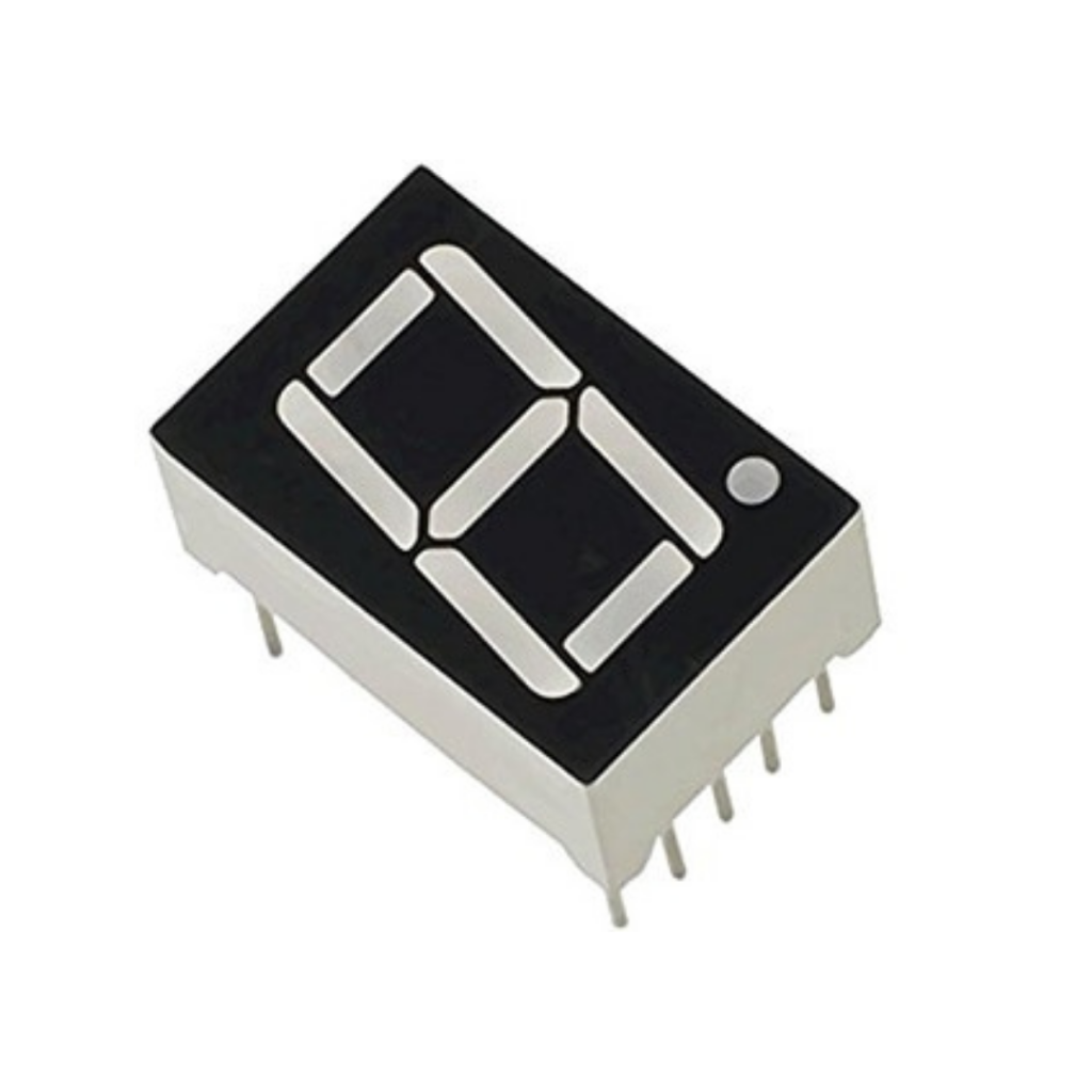
1. What is 7 Segment Display:
A 7-segment display is an electronic display device used to show decimal numerals. It’s an alternative to more complex dot matrix displays. Here are the key points about 7-segment displays:
- Structure:
- A 7-segment display consists of seven LEDsarranged in a rectangular fashion.
- Each LED is called a segment because when illuminated, it forms part of a numerical digit (both decimal and hexadecimal) to be displayed.
- An additional 8th LED is sometimes included within the same package to indicate a decimal point (DP) when multiple 7-segment displays are connected together to display numbers greater than ten.
- Working Principle:
- When the diode junction of each segment is forward biased by an external voltage, it allows current to flow across its junction, resulting in the emission of light.
- The actual color of the visible light emitted by an LED (ranging from blue to red to orange) depends on the spectral wavelength of the emitted light, which itself is influenced by the mixture of impurities added to the semiconductor materials used to produce it.
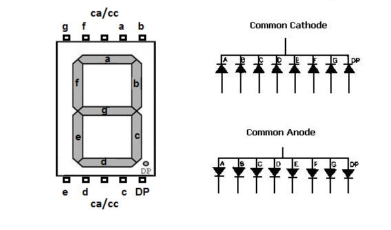
- Common Types:
- There are two common types of LED 7-segment displays:
- Common Cathode (CC): All cathodes of the 7-segments are connected directly together.
- Common Anode (CA): All anodes of the 7-segments are connected together.
- There are two common types of LED 7-segment displays:
- Displaying Numbers:
- By forward biasing the appropriate pins of the LED segments in a specific order, some segments will be lit, while others remain dark.
- This allows us to display each of the ten decimal digits (0 through 9) on the same 7-segment display.
- Applications:
- 7-segment displays are widely used in various devices, including:
- Digital clocks
- Electronic meters
- Basic calculators
- 7-segment displays are widely used in various devices, including:
2. Connection of Common Anode with STM32F4xx:
The connection as following:

Connect A to G from the display to PC0 to PC6 on the STM32F4xx. Here, we don’t need the DP (Decimal Point).
Connect the 3.3V through 220Ohm resistor to the Common anode. In case you have common cathode, connect the port to ground through 220Ohm resistor.
3. Developing the Driver:
Before heading into the driver, take a look at this guide for how to configure the timer to generate DMA to control the GPIO.
We start off by including the main STM32F4 header file as following:
#include "stm32f4xx.h"
Since the size of the array to hold the number from 0 to 9 is 10, we shall create a macro for it as following:
#define data_size 10
For the DMA channel, it should be channel 6:
#define CH6 0x06
Here, we are defining if we are using common anode or common cathode:
#define COMMOM_ANODE 1
In case of common cathode, just define it as zero.
Here is the array to hold the state of the pins to display certain number:
#if COMMOM_ANODE


const uint32_t seven_segment_lookup[] = {

	    0b11000000, // 0
	    0b11111001, // 1
	    0b10100100, // 2
	    0b10110000, // 3
	    0b10011001, // 4
	    0b10010010, // 5
	    0b10000010, // 6
	    0b11111000, // 7
	    0b10000000, // 8
	    0b10010000  // 9
};

#else

const uint32_t seven_segment_lookup[] = {
	    0b00111111, // 0
	    0b00000110, // 1
	    0b01011011, // 2
	    0b01001111, // 3
	    0b01100110, // 4
	    0b01101101, // 5
	    0b01111101, // 6
	    0b00000111, // 7
	    0b01111111, // 8
	    0b01101111  // 9

};

#endif
The rest of the code is similar to the parallel port emulation:
int main(void)
{
	/*GPIO Configuration*/

	/*Enable clock access to GPIOA*/
	RCC->AHB1ENR|=RCC_AHB1ENR_GPIOCEN;

	/*Set PC0 to PC7 as output*/
	GPIOC->MODER|=GPIO_MODER_MODE0_0|GPIO_MODER_MODE1_0|GPIO_MODER_MODE2_0
			|GPIO_MODER_MODE3_0|GPIO_MODER_MODE4_0|GPIO_MODER_MODE5_0|
			GPIO_MODER_MODE6_0|GPIO_MODER_MODE7_0;

	GPIOC->MODER&=~(GPIO_MODER_MODE0_1|GPIO_MODER_MODE1_1|GPIO_MODER_MODE2_1
			|GPIO_MODER_MODE3_1|GPIO_MODER_MODE4_1|GPIO_MODER_MODE5_1
			|GPIO_MODER_MODE6_1|GPIO_MODER_MODE7_1);


	/*Timer configuration*/

	RCC->APB2ENR  |=  RCC_APB2ENR_TIM1EN;

	TIM1->DIER=TIM_DIER_UDE;

	TIM1->PSC=16000-1; /*16 000 000 / 16 000 =1 000*/
	TIM1->ARR=1000-1; /*1 000 / 1 000 = 1HZ*/


	/*DMA configuration*/


	RCC->AHB1ENR|=RCC_AHB1ENR_DMA2EN;

	DMA2_Stream5->CR&=DMA_SxCR_EN;

	while((DMA2_Stream5->CR)&DMA_SxCR_EN){;}

	DMA2_Stream5->CR|=(CH6<<DMA_SxCR_CHSEL_Pos)|DMA_SxCR_MSIZE|DMA_SxCR_PSIZE|
			DMA_SxCR_MINC|DMA_SxCR_CIRC|DMA_SxCR_DIR_0;

	DMA2_Stream5->NDTR=(uint32_t)data_size;

	DMA2_Stream5->PAR=(uint32_t)(&GPIOC->ODR);

	DMA2_Stream5->M0AR=(uint32_t)(seven_segment_lookup);


	/*Launch DMA*/
	DMA2_Stream5->CR|=DMA_SxCR_EN;

	/*Launch Timer*/
	TIM1->CR1     |= TIM_CR1_CEN;


	while(1)
	{

	}

}
Hence, the entire code as following:
#include "stm32f4xx.h"


#define data_size 	10
#define CH6 		0x06

#define COMMOM_ANODE 1


#if COMMOM_ANODE


const uint32_t seven_segment_lookup[] = {

	    0b11000000, // 0
	    0b11111001, // 1
	    0b10100100, // 2
	    0b10110000, // 3
	    0b10011001, // 4
	    0b10010010, // 5
	    0b10000010, // 6
	    0b11111000, // 7
	    0b10000000, // 8
	    0b10010000  // 9
};

#else

const uint32_t seven_segment_lookup[] = {
	    0b00111111, // 0
	    0b00000110, // 1
	    0b01011011, // 2
	    0b01001111, // 3
	    0b01100110, // 4
	    0b01101101, // 5
	    0b01111101, // 6
	    0b00000111, // 7
	    0b01111111, // 8
	    0b01101111  // 9

};

#endif


int main(void)
{
	/*GPIO Configuration*/

	/*Enable clock access to GPIOA*/
	RCC->AHB1ENR|=RCC_AHB1ENR_GPIOCEN;

	/*Set PC0 to PC7 as output*/
	GPIOC->MODER|=GPIO_MODER_MODE0_0|GPIO_MODER_MODE1_0|GPIO_MODER_MODE2_0
			|GPIO_MODER_MODE3_0|GPIO_MODER_MODE4_0|GPIO_MODER_MODE5_0|
			GPIO_MODER_MODE6_0|GPIO_MODER_MODE7_0;

	GPIOC->MODER&=~(GPIO_MODER_MODE0_1|GPIO_MODER_MODE1_1|GPIO_MODER_MODE2_1
			|GPIO_MODER_MODE3_1|GPIO_MODER_MODE4_1|GPIO_MODER_MODE5_1
			|GPIO_MODER_MODE6_1|GPIO_MODER_MODE7_1);


	/*Timer configuration*/

	RCC->APB2ENR  |=  RCC_APB2ENR_TIM1EN;

	TIM1->DIER=TIM_DIER_UDE;

	TIM1->PSC=16000-1; /*16 000 000 / 16 000 =1 000*/
	TIM1->ARR=1000-1; /*1 000 / 1 000 = 1HZ*/


	/*DMA configuration*/


	RCC->AHB1ENR|=RCC_AHB1ENR_DMA2EN;

	DMA2_Stream5->CR&=DMA_SxCR_EN;

	while((DMA2_Stream5->CR)&DMA_SxCR_EN){;}

	DMA2_Stream5->CR|=(CH6<<DMA_SxCR_CHSEL_Pos)|DMA_SxCR_MSIZE|DMA_SxCR_PSIZE|
			DMA_SxCR_MINC|DMA_SxCR_CIRC|DMA_SxCR_DIR_0;

	DMA2_Stream5->NDTR=(uint32_t)data_size;

	DMA2_Stream5->PAR=(uint32_t)(&GPIOC->ODR);

	DMA2_Stream5->M0AR=(uint32_t)(seven_segment_lookup);


	/*Launch DMA*/
	DMA2_Stream5->CR|=DMA_SxCR_EN;

	/*Launch Timer*/
	TIM1->CR1     |= TIM_CR1_CEN;


	while(1)
	{

	}

}
4. Results:
Once you compiled and run the code on STM32, this should be the results.
Happy coding 🙂
2 Comments
Good afternoon. Good post, I tried everything, it works. But I didn’t understand the most important thing: what causes cyclic reading in this line of code
DMA2_Stream5->M0AR = (uint32_t) (seven_segment_lookup);
Hi,
the DMA is configured in circular mode. Once the data have been transferred, the DMA will start transfer again from the start of the array.
This is the nature of DMA in circular mode.
Add Comment