In the previous guide (here), we discussed how to use the timer to generate accurate delay. In this guide, we shall look at another application for timer which is to generate PWM signal on two channels and fading two leds.
In this guide, we will cover the following:
- What is PWM
- Configure the timer and GPIO to generate PWM signal
- Connection
- Code
- Demo
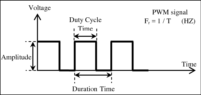
1. What is PWM:
PWM is a technique used to emulate “analog signal” by rapidly turning on-off the pin. This allow the mcu to vary the power delivered to the load such as motor (will be covered later). The PWM has three main characteristics;
- Frequency:
which describe the duration time of the entire signal
- Duty cycle
The term duty cycle describes the proportion of ‘on’ time to the regular interval or ‘period’ of time; a low duty cycle corresponds to low power, because the power is off for most of the time. Duty cycle is expressed in percent, 100% being fully on.
- Amplitude
Which is the voltage level of the PWM (3.3v for STM32F7).
For more details, please check this wikipedia article (here)
2. Configure the timer and GPIO to generate PWM Signal:
First we need to locate which pins connected to TIMER2_CH1 and TIMER2_CH2.
From the datasheet, we can find the related timer channels
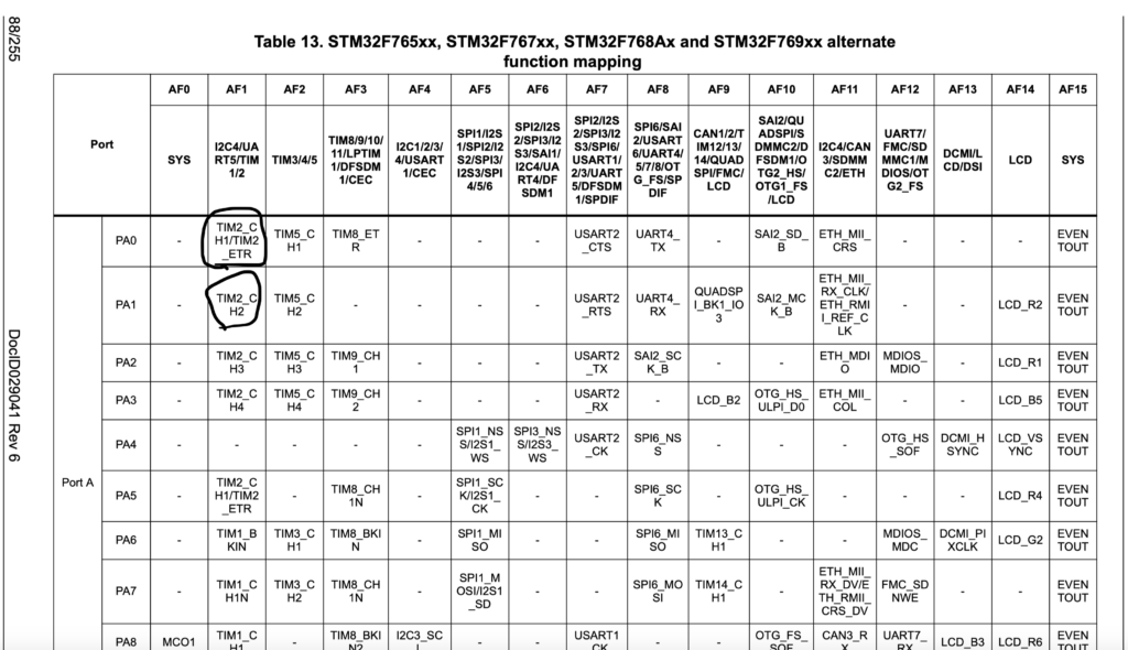
From the datasheet, we can see that TIM2_CH1 is connected to PA0 and CH2 is connected to PA1.
Hence, we can start configuring the timer and GPIO
We start off by setting GPIO
First thing first, we need to enable clock access to GPIOA as following: (for enabling clock access, check this topic)
RCC->AHB1ENR|=RCC_AHB1ENR_GPIOAEN;
Then setting the pins in alternate mode as following:
GPIOA->MODER&=~	GPIO_MODER_MODER0|GPIO_MODER_MODER1; //reset PA0 and PA1
GPIOA->MODER|=	GPIO_MODER_MODER0_1|GPIO_MODER_MODER1_1; //set PA0 and PA1 as alternate mode
Then select which alternate function, in our case it is AF1
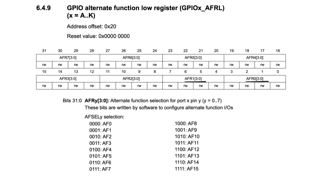
#define AF01 0x01
GPIOA->AFR[0]|=(AF01<<0)|(AF01<<4);
Now we can configure the timer to generate PWM signal
We start off by enabling clock access to TIMER2 as following:
RCC->APB1ENR|=RCC_APB1ENR_TIM2EN; //enable clock access to tim2
Set the prescaller to 0 (no divider)
TIM2->PSC=0; //set prescaller to 0 (no divider)
Set the maximum value to 255 ( this will give frequency of 62.5KHz)
TIM2->ARR=255; //set the maximum count value
Reset the current counter
TIM2->CNT=0; //reset the current count
Now, we configure the mode to be PWM mode as following:
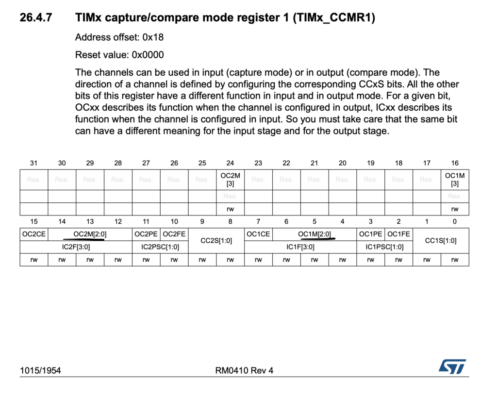
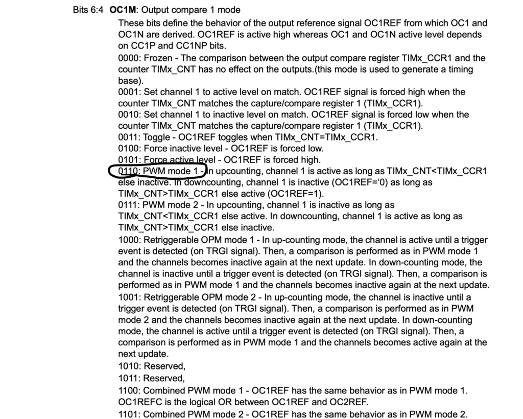
TIM2->CCMR1=TIM_CCMR1_OC1M_1|TIM_CCMR1_OC1M_2|TIM_CCMR1_OC2M_1|TIM_CCMR1_OC2M_2; //configure the pins as PWM
And enable the channel as following:
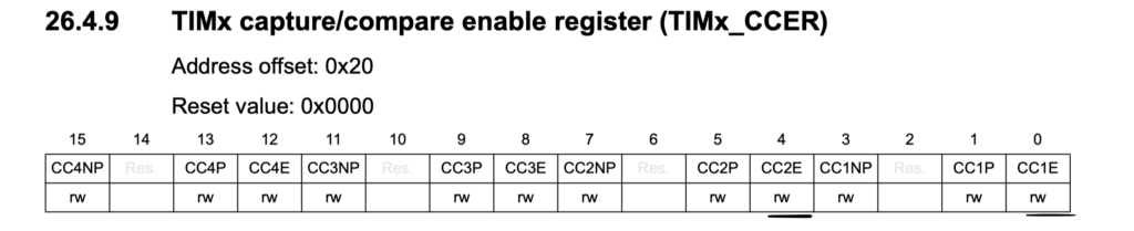
TIM2->CCER|=TIM_CCER_CC1E|TIM_CCER_CC2E; //enbale channel1 and channel2
Finally, we enable the timer as following:
TIM2->CR1=TIM_CR1_CEN; //enable timer
hence, the initializing function shall be this
void GPIO_Init(void)
{
#define AF01 0x01
RCC->AHB1ENR|=	RCC_AHB1ENR_GPIOAEN;// enable clock access
GPIOA->MODER&=~	GPIO_MODER_MODER0|GPIO_MODER_MODER1; //reset PA0 and PA1
GPIOA->MODER|=	GPIO_MODER_MODER0_1|GPIO_MODER_MODER1_1; //set PA0 and PA1 as alternate mode

GPIOA->AFR[0]|=(AF01<<0)|(AF01<<4);


}
void  Timer2_init(void){
RCC->APB1ENR|=RCC_APB1ENR_TIM2EN; //enable clock access to tim2
TIM2->PSC=0; //set prescaller to 0 (no divider)
TIM2->ARR=255; //set the maximum count value
TIM2->CNT=0; //reset the current count
TIM2->CCMR1=TIM_CCMR1_OC1M_1|TIM_CCMR1_OC1M_2|TIM_CCMR1_OC2M_1|TIM_CCMR1_OC2M_2; //configure the pins as PWM
TIM2->CCER|=TIM_CCER_CC1E|TIM_CCER_CC2E; //enbale channel1 and channel2
TIM2->CR1=TIM_CR1_CEN; //enable timer
}
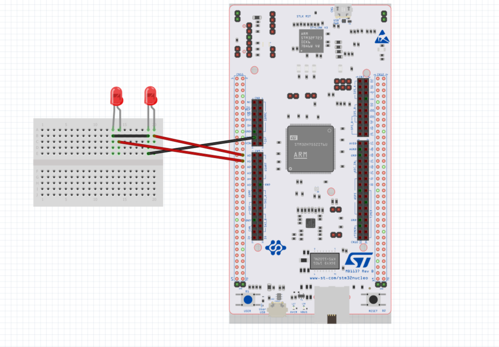
3. Connection:
4. Code:
#include "stm32f7xx.h"                  // Device header
void GPIO_Init(void);
void Timer2_init(void);
void delay(int ms );
#define rate 255
int main(void)
{

GPIO_Init();
Timer2_init();
while(1)
{
for (int i=0;i<rate;i++){
TIM2->CCR1=i;
TIM2->CCR2=rate-i;
delay(2);
}
for (int i=255;i>0;i--){
TIM2->CCR1=i;
TIM2->CCR2=rate-i;
delay(2);
}

}
}

void GPIO_Init(void)
{
#define AF01 0x01
RCC->AHB1ENR|=	RCC_AHB1ENR_GPIOAEN;// enable clock access
GPIOA->MODER&=~	GPIO_MODER_MODER0|GPIO_MODER_MODER1; //reset PA0 and PA1
GPIOA->MODER|=	GPIO_MODER_MODER0_1|GPIO_MODER_MODER1_1; //set PA0 and PA1 as alternate mode

GPIOA->AFR[0]|=(AF01<<0)|(AF01<<4);


}
void  Timer2_init(void){
RCC->APB1ENR|=RCC_APB1ENR_TIM2EN; //enable clock access to tim2
TIM2->PSC=0; //set prescaller to 0 (no divider)
TIM2->ARR=255; //set the maximum count value
TIM2->CNT=0; //reset the current count
TIM2->CCMR1=TIM_CCMR1_OC1M_1|TIM_CCMR1_OC1M_2|TIM_CCMR1_OC2M_1|TIM_CCMR1_OC2M_2; //configure the pins as PWM
TIM2->CCER|=TIM_CCER_CC1E|TIM_CCER_CC2E; //enbale channel1 and channel2
TIM2->CR1=TIM_CR1_CEN; //enable timer
}


void delay(int ms)

{

volatile int i;

for(; ms>0 ;ms--)

{

for(i =0; i<3195;i++);

}

}
5. Demo:
Happy coding 😀
6 Comments
TIM2->CCMR1=TIM_CCMR1_OC1M_1|TIM_CCMR1_OC1M_2|TIM_CCMR1_OC2M_1|TIM_CCMR1_OC2M_2; //configure the pins as PWM
——————————————————————————————————————————————–
TIM2->CCMR1 | =
Why is there no or operator?
You can use either | or =.
The | will modify only the required bits from 0 to 1 while = will set the entire register to the desired value.
Mr Husamuldeen, for your answer Thank you
I live in Turkey, Whenever I have time, I learn from the articles you write on your website.I am interested in programming as a hobby.I do other jobs for a living.age 51
see you goodbye
Nothing I am aware of.
It should just be the SPI function and the delay function that needed to be changed.
TIM2->CCMR1=
TIM_CCMR1_OC1M_1 | TIM_CCMR1_OC1M_2|
TIM_CCMR1_OC2M_1 | TIM_CCMR1_OC2M_2;
I couldn’t see any value assigned to the first and second bits of OC1M.
Hi,
Is the PWM working properly ?
Add Comment