In this new guide series, we shall see how to interface W25QXX External flash memory with STM32F4xx using SPI.
In this guide, we shall cover the following:
- W25Qxx Feature.
- Developing the SPI driver.
- Developing the delay driver.
- Connection with STM32F4xx
- Developing the W25QXX driver.
- Main code.
- Results.
1. W25QXX Features:
The W25Q32JV (32M-bit) Serial Flash memory provides a storage solution for systems with limited space, pins and power. The 25Q series offers flexibility and performance well beyond ordinary Serial Flash devices. They are ideal for code shadowing to RAM, executing code directly from Dual/Quad SPI (XIP) and storing voice, text and data. The device operates on 2.7V to 3.6V power supply with current consumption as low as 1µA for power-down.
The W25Q32JV array is organized into 16,384 programmable pages of 256-bytes each. Up to 256 bytes can be programmed at a time. Pages can be erased in groups of 16 (4KB sector erase), groups of 128 (32KB block erase), groups of 256 (64KB block erase) or the entire chip (chip erase). The W25Q32JV has 1,024 erasable sectors and 64 erasable blocks respectively. The small 4KB sectors allow for greater flexibility in applications that require data and parameter storage. (See Figure 2.)
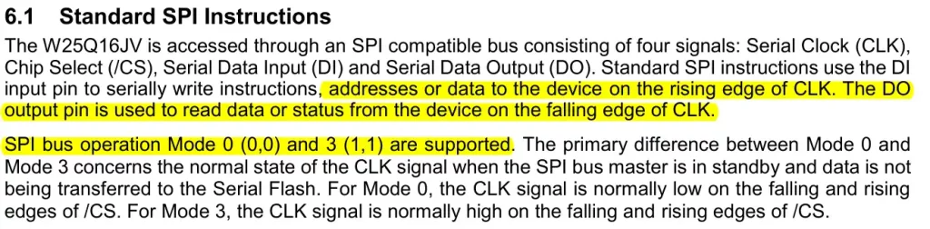
The W25Q32JV supports the standard Serial Peripheral Interface (SPI), and a high performance Dual/Quad output as well as Dual/Quad I/O SPI: Serial Clock, Chip Select, Serial Data I/O0 (DI), I/O1 (DO), I/O2, and I/O3. SPI clock frequencies of up to 133MHz are supported allowing equivalent clock rates of 266MHz (133MHz x 2) for Dual I/O and 532MHz (133MHz x 4) for Quad I/O when using the Fast Read Dual/Quad I/O instructions. These transfer rates can outperform standard Asynchronous 8 and 16-bit Parallel Flash memories.
Additionally, the device supports JEDEC standard manufacturer and device ID and SFDP Register, a 64bit Unique Serial Number and three 256-bytes Security Registers.
FEATURES
New Family of SpiFlash Memories
– W25Q32JV: 32M-bit / 4M-byte
– Standard SPI: CLK, /CS, DI, DO
Flexible Architecture with 4KB sectors
– Uniform Sector/Block Erase (4K/32K/64K-Byte)
– Program 1 to 256 byte per programmable page
– Dual SPI: CLK, /CS, IO0 , IO1
– Quad SPI: CLK, /CS, IO0 , IO1 , IO2 , IO3
– Software & Hardware Reset(1)
Highest Performance Serial Flash
– 133MHz Single, Dual/Quad SPI clocks
– 266/532MHz equivalent Dual/Quad SPI
– 66MB/S continuous data transfer rate
– Min. 100K Program-Erase cycles per sector
– More than 20-year data retention
Efficient “Continuous Read”
– Continuous Read with 8/16/32/64-Byte Wrap
– As few as 8 clocks to address memory
– Allows true XIP (execute in place) operation
– Outperforms X16 Parallel Flash
Low Power, Wide Temperature Range
– Single 2.7V to 3.6V supply
– <1µA Power-down (typ.)
– -40°C to +85°C operating range
– Erase/Program Suspend & Resume
Advanced Security Features
– Software and Hardware Write-Protect
– Special OTP protection(2)
– Top/Bottom, Complement array protection
– Individual Block/Sector array protection
– 64-Bit Unique ID for each device
– Discoverable Parameters (SFDP) Register
– 3X256-Bytes Security Registers
– Volatile & Non-volatile Status Register Bits
Pin out:

2. Developing SPI Driver:
Before we start with drivers, take a look here what is SPI and how to enable clock access etc and related pins.
Also, check
We start off by creating new header file with name of SPI1.h.
Within the header file, include header guard as following:
#ifndef SPI1_H_
#define SPI1_H_


#endif /* SPI1_H_ */
Within the header guard, in the stdint library as following:
#include "stdint.h"
Declare the following functions:
void SPI1_Pins_Init(void);
This function will initialize the SPI1 related pins (PA5, PA6 and PA7) and take no argument and returns nothing.
void W25QXX_CS_Pins_Init(void);
This function will initialize the CS pin (PA0) and set to default state of high, it takes no argument and returns nothing.
void SPI1_Config(void);
This will configure the SPI, it takes no argument and returns nothing.
void SPI1_Transmit(uint8_t *data,uint32_t size);
This function will transmit data over the SPI bus, it takes pointer to array that holds the data to be written and size of the array and returns nothing.
void SPI1_Receive(uint8_t *data,uint32_t size);
This function will receive bytes from the SPI bus, it takes pointer to array to store the received data and size of the data to be received.
void W25QXX_CS_LOW(void);

void W25QXX_CS_HIGH(void);
These two functions will set/reset the CS pin according to the SPI requirements. Both functions take no argument and return nothing.
Now, create new source file with name of SPI1.c.
Within the source file, include the following:
#include <SPI1.h>
#include "stm32f4xx.h"
Include the SPI1 header file and main STM32F4xx header file.
For SPI GPIO initialization function:
void SPI1_Pins_Init(void)
{
	RCC->AHB1ENR|=RCC_AHB1ENR_GPIOAEN; //enable clock for GPIOA
	GPIOA->MODER|=GPIO_MODER_MODE5_1|GPIO_MODER_MODE6_1|GPIO_MODER_MODE7_1; //set PA5, PA6 and PA7 to alternate function mode
	GPIOA->MODER &=~(GPIO_MODER_MODE5_0|GPIO_MODER_MODE6_0|GPIO_MODER_MODE7_0);

	GPIOA->OSPEEDR|=GPIO_OSPEEDER_OSPEEDR5|GPIO_OSPEEDER_OSPEEDR6|GPIO_OSPEEDER_OSPEEDR7;

	GPIOA->AFR[0]|=(0x05<<20)|(0x05<<24)|(0x05<<28);
}
For the CS pin:
void W25QXX_CS_Pins_Init(void)
{
	RCC->AHB1ENR|=RCC_AHB1ENR_GPIOAEN; //enable clock for GPIOA
	/*Set PA0 as output*/
	GPIOA->MODER|=GPIO_MODER_MODE0_0;
	GPIOA->MODER&=~GPIO_MODER_MODE0_1;

	/*Set pin high as initial state*/
	GPIOA->BSRR =GPIO_BSRR_BS0;
}
The SPI shall be configured with the following parameters:
- CPOL and CPHA 0 (Mode0).
- Master mode.
- Software slave management.
- MSB first.
void SPI1_Config(void)
{
	/*Enable clock access to SPI1 module*/
	RCC->APB2ENR |= RCC_APB2ENR_SPI1EN;

	/*Set clock to fPCLK/2*/
	SPI1->CR1 &=~SPI_CR1_BR_0;
	SPI1->CR1 &=~SPI_CR1_BR_1;
	SPI1->CR1 &=~SPI_CR1_BR_2;

	/*Set CPOL to 0 and CPHA to 0 (MODE0)*/
	SPI1->CR1 &=~(SPI_CR1_CPOL);
	SPI1->CR1 &=~(SPI_CR1_CPHA);

	/*Enable full duplex*/
	SPI1->CR1 &=~(SPI_CR1_RXONLY);

	/*Set MSB first*/
	SPI1->CR1 &= ~(SPI_CR1_LSBFIRST);

	/*Set mode to MASTER*/
	SPI1->CR1 |= (SPI_CR1_MSTR);

	/*Set 8 bit data mode*/
	SPI1->CR1 &= ~(SPI_CR1_DFF);

	/*Select software slave management by
	* setting SSM=1 and SSI=1*/
	SPI1->CR1 |= (SPI_CR1_SSM);
	SPI1->CR1 |= (SPI_CR1_SSI);

	/*Enable SPI module*/
	SPI1->CR1 |= (SPI_CR1_SPE);
}
For SPI transmit:
void SPI1_Transmit(uint8_t *data,uint32_t size)
{
	uint32_t i=0;

	while(i<size)
	{
		/*Wait until TXE is set*/
		while(!(SPI1->SR & (SPI_SR_TXE))){}

		/*Write the data to the data register*/
		SPI1->DR = data[i];
		i++;
	}
	/*Wait until TXE is set*/
	while(!(SPI1->SR & (SPI_SR_TXE))){}

	/*Wait for BUSY flag to reset*/
	while((SPI1->SR & (SPI_SR_BSY))){}

	/*Clear OVR flag*/
	(void)SPI1->DR;
	(void)SPI1->SR;
}
For SPI receive:
void SPI1_Receive(uint8_t *data,uint32_t size)
{
	while(size)
	{
		/*Send dummy data*/
		SPI1->DR =0;

		/*Wait for RXNE flag to be set*/
		while(!(SPI1->SR & (SPI_SR_RXNE))){}

		/*Read data from data register*/
		*data++ = (SPI1->DR);
		size--;
	}
}
CS state:
void W25QXX_CS_LOW(void)
{
	GPIOA->BSRR =GPIO_BSRR_BR0;

}

/*Pull high to disable*/
void W25QXX_CS_HIGH(void)
{
	GPIOA->BSRR =GPIO_BSRR_BS0;
}
Thats all for the SPI part.
3. Developing the Delay Driver:
With delay, we shall use SysTick to generate interrupt each 1 milliseconds.
Check this guide for how to generate interrupt using systick.
Create new header file with name of delay.h.
The header file as following:
#ifndef __delay__H__
#define __delay__H__

#include "stdint.h"

void delay_init(uint32_t freq);
uint64_t millis();
void delay(uint32_t time);


#endif
Create new source file with name of delay.c.
The content of delay as following:
#include "delay.h"
#include "stm32f4xx.h"


#define	CTRL_ENABLE					(1U<<0)
#define CTRL_CLKSRC					(1U<<2)
#define CTRL_COUNTFLAG				(1U<<16)
#define CTRL_TICKINT				(1U<<1)


volatile uint64_t mil;

void delay_init(uint32_t freq)
{

	SysTick->LOAD  = (freq/1000) - 1;

	/*Clear systick current value register */
	SysTick->VAL = 0;

	/*Enable systick and select internal clk src*/
	SysTick->CTRL = CTRL_ENABLE | CTRL_CLKSRC ;

	/*Enable systick interrupt*/
	SysTick->CTRL  |= CTRL_TICKINT;

}


uint64_t millis()
	{
	__disable_irq();
	uint64_t ml=mil;
	__enable_irq();
	return ml;
	}


void delay(uint32_t time)
{

	uint64_t start=millis();
	while((millis() - start) < (time+1));
}

void SysTick_Handler(void)
{

	mil++;
}
4. Connection with STM32F4xx:
The connection as following:

| STM32F411-Nucleo64 | W25QXX |
| 3V3 | Vcc |
| GND | GND |
| PA0 | CS |
| PA5 | CLK |
| PA6 | DO |
| PA7 | DI |
Note: Chip only supports 3v3, powering it from 5V will destroy it.
5. Developing W25QXX driver:
Create new header file with name of W25QXX.h
Within the header file, include the header guard:
#ifndef W25QXX_H_
#define W25QXX_H_


#endif /* W25QXX_H_ */
Within the header guard, include the stdint:
#include "stdint.h"
Declare the following functions:
void W25QXX_Reset(void);
This function will soft reset the flash and takes no argument and returns nothing.
uint32_t W25QXX_ReadID (void);
This function will read the ID of the chip and takes no argument and return the ID as uint32_t value.
Hence, the header file as following:
#ifndef W25QXX_H_
#define W25QXX_H_

#include "stdint.h"

void W25QXX_Reset(void);

uint32_t W25QXX_ReadID (void);


#endif /* W25QXX_H_ */
Create new source file with name of W25QXX.c.
Within the source file, include the following:
#include "W25QXX.h"

#include "SPI1.h"
For the reset, we need to send two commands one after the another as mentioned in the datasheet:

Hence, the reset function as following:
void W25QXX_Reset(void)
{
declare an array that hold two variable:
uint8_t tData[2];
Define the two values for reset enable and reset:
tData[0] = 0x66;  // enable Reset
tData[1] = 0x99;  // Reset
Transmit the data:
	W25QXX_CS_LOW();
	SPI1_Transmit(tData, 2);
	W25QXX_CS_HIGH();
Hence the function as following:
void W25QXX_Reset(void)
{
	uint8_t tData[2];

	tData[0] = 0x66;  // enable Reset
	tData[1] = 0x99;  // Reset
	W25QXX_CS_LOW();
	SPI1_Transmit(tData, 2);
	W25QXX_CS_HIGH();
}
To read the ID, we simply send 0x9F and receive the three bytes that contain the ID and size as following:

uint32_t W25QXX_ReadID (void)
{
Declare a variable to hold the read command as following:
uint8_t tData = 0x9f; // Read ID
Declare an array to hold the ID as following:
uint8_t rData[3];
Transmit and receive data as following:
	W25QXX_CS_LOW();
	SPI1_Transmit(&tData,1);
	SPI1_Receive(rData, 3);
	W25QXX_CS_HIGH();
Return the data:
return ((rData[0]<<16)|(rData[1]<<8)|rData[2]); // MFN ID : MEM ID : CAPACITY ID
Hence the function as following:
uint32_t W25QXX_ReadID (void)
{
	uint8_t tData = 0x9f;  // Read ID
	uint8_t rData[3];
	W25QXX_CS_LOW();
	SPI1_Transmit(&tData,1);
	SPI1_Receive(rData, 3);
	W25QXX_CS_HIGH();

	return ((rData[0]<<16)|(rData[1]<<8)|rData[2]); // MFN ID : MEM ID : CAPACITY ID
}
The source file as following:
#include "W25QXX.h"

#include "SPI1.h"


void W25QXX_Reset(void)
{
	uint8_t tData[2];

	tData[0] = 0x66;  // enable Reset
	tData[1] = 0x99;  // Reset
	W25QXX_CS_LOW();
	SPI1_Transmit(tData, 2);
	W25QXX_CS_HIGH();
}

uint32_t W25QXX_ReadID (void)
{
	uint8_t tData = 0x9f;  // Read ID
	uint8_t rData[3];
	W25QXX_CS_LOW();
	SPI1_Transmit(&tData,1);
	SPI1_Receive(rData, 3);
	W25QXX_CS_HIGH();

	return ((rData[0]<<16)|(rData[1]<<8)|rData[2]); // MFN ID : MEM ID : CAPACITY ID
}
6. Main.c code:
The code within main.c:
#include "delay.h"
#include "SPI1.h"
#include "W25QXX.h"

uint32_t W25QXX_ID;


int main(void)
{	delay_init(16000000);

	SPI1_Pins_Init();
	W25QXX_CS_Pins_Init();
	SPI1_Config();

	W25QXX_Reset();
	delay(10);

	W25QXX_ID=W25QXX_ReadID();


	while(1)
	{


	}

}
7. Results:
Upload the code to your MCU and open a debugging session and add W25QXX_ID to expression value and run the code. You should get the EF for winbond serial flash and model number (W25Q32 in this case)

Happy coding 🙂
2 Comments
how to interface w25q32 flash with stm32 using stmcubeide and fatfs.
i want to link fatfs and spi commands and create file system on w25q32 like sd card.how can i done it.
FatFS is designed for SD-Cards etc.
Using with this type of flash is pointless. Usually, this type of flash holds either the firmware or part of the code where it needs large fixed data like images etc.
Add Comment