
In this guide, we shall develop driver to measure the frequency and duty cycle of a signal.
In this guide, we shall cover the following:
- What is PWM input mode.
- Required steps.
- Driver.
- STM32 Connection
- Code.
- Results.
1. What is PWM Input Mode:
PWM input mode is similar to input capture mode (explained here) with the following differences:
Two ICx signals are mapped on the same TIx input.
These 2 ICx signals are active on edges with opposite polarity.
One of the two TIxFP signals is selected as trigger input and the slave mode controller is configured in reset mode.
For example, one can measure the period (in TIMx_CCR1 register) and the duty cycle (in TIMx_CCR2 register) of the PWM applied on TI1.
The timing diagram as following:
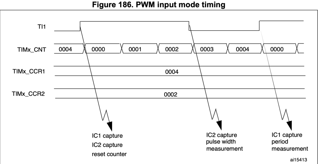
When an rising edge is detected, the IC1 is capture and IC2 is reset. When fall edge is detected, IC2 capture the duty cycle (pulse width). The cycles continues.
To measure the frequency, the following equation can be used:

For the duty cycle:

That all for the theory of PWM input mode.
2. Required steps:
The required steps as following:
3. Developing the Driver:
This guide shall use timer2 to measure the frequency and duty cycle of a signal applied to PA0 and PWM signal generated from PA8 connected to TIM1. For timer 1 PWM generation, please refer to this guide. Also, the core is set to 100MHz from here.
Since the signal is connected to PA0 and this pin is connected to TIM2, we shall enable clock access to GPIOA as following:
	/*Enable clock access to GPIOA*/
	RCC->AHB1ENR|=RCC_AHB1ENR_GPIOAEN;
Set PA0 to alternate function and select which alternate function as following:
	/*Set PA0 and PA1 to alternate function*/
	GPIOA->MODER|=(GPIO_MODER_MODE0_1);
	GPIOA->MODER&=~(GPIO_MODER_MODE0_0);

	/*Select AF01 for TIM2*/
	#define AF01 0x01
	GPIOA->AFR[0]|=(AF01<<GPIO_AFRL_AFSEL0_Pos)|(AF01<<GPIO_AFRL_AFSEL1_Pos);
Thats all for the GPIO configuration, next timer configuration.
We start off by enabling clock access to TIM2 (please refer to this guide for more details how to enable clock access):
	/*enable clock access to tim2*/
	RCC->APB1ENR|=RCC_APB1ENR_TIM2EN;
Set prescaller to 0 to get full speed:
	/*set the prescaler to 0 to get 100MHZ*/
	TIM2->PSC=0;
Set the Auto reload value to maximum (32-bit value):
	/*set the maximum to 199999 to get 5 Hz update rate*/
	TIM2->ARR=0xFFFFFFFF;
Reset the counter:
	/*Reset current counter*/
	TIM2->CNT=0;
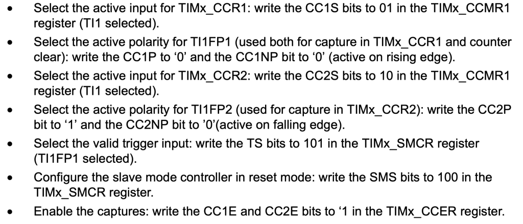
Set CH1 to input mapped to TI1 as following:
	/*Set TIM2_Ch1 to be input mapped to TI1*/
	TIM2->CCMR1|=TIM_CCMR1_CC1S_0;
Set the trigger to be rising edge:
	/*Select TIM2 CH1 to be Rising edge*/
	TIM2->CCER&=~(TIM_CCER_CC1P|TIM_CCER_CC1NP);
Set CH2 as input mapped to TI1 as following:
	/*Set TIM2_CH2 to be input mapped to TI1*/
	TIM2->CCMR1|=TIM_CCMR1_CC2S_1;
Set the detection edge to be falling edge:
	/*Select TIM2 CH1 to be Falling edge*/
	TIM2->CCER|=TIM_CCER_CC2P;
	TIM2->CCER&=~TIM_CCER_CC2NP;
Set trigger mode to be filtered Timer Input 1 as following:
	/*Set trigger mode to be Filtered Timer Input 1*/
	TIM2->SMCR|=TIM_SMCR_TS_2|TIM_SMCR_TS_0;
Set the slave mode to be reset mode:
	/*Set the slave mode to be reset mode*/
	TIM2->SMCR|=TIM_SMCR_SMS_2;
Enable both channel:
	/*Enable both channel*/
	TIM2->CCER|=TIM_CCER_CC1E|TIM_CCER_CC2E;
Enable DMA for both channel as following:
	/*Enable DMA for both channel*/

	TIM2->DIER|=TIM_DIER_CC1DE|TIM_DIER_CC2DE;
For DMA configuration (covered here):
/*DMA configuration*/ /*Enable clock access to DMA1*/ RCC->AHB1ENR|=RCC_AHB1ENR_DMA1EN; /*Disable the stream and wait until it is disabled*/ DMA1_Stream6->CR &=~DMA_SxCR_EN; while((DMA1_Stream6->CR & DMA_SxCR_EN) == DMA_SxCR_EN ); /*Configure the DMA with the following parameters * * Channel is channel 3 * Memory and peripheral size is word (32-bit) * Circular mode * * */ #define CH3 0x03 DMA1_Stream6->CR |= (CH3<<DMA_SxCR_CHSEL_Pos)|DMA_SxCR_PSIZE_1|DMA_SxCR_MSIZE_1|DMA_SxCR_CIRC; /*Set number of transfers to be 1 * Peripheral address to TIM2->CCR2 * Memory address to be the period variable * */ DMA1_Stream6->NDTR=1; DMA1_Stream6->PAR= (uint32_t)&TIM2->CCR2; DMA1_Stream6->M0AR=(uint32_t)&duty_cycle; /*Enable DMA*/ DMA1_Stream6->CR |=DMA_SxCR_EN; /*Disable the stream and wait until it is disabled*/ DMA1_Stream5->CR &=~DMA_SxCR_EN; while((DMA1_Stream5->CR & DMA_SxCR_EN) == DMA_SxCR_EN ); /*Configure the DMA with the following parameters * * Channel is channel 3 * Memory and peripheral size is word (32-bit) * Circular mode * * */ DMA1_Stream5->CR |= (CH3<<DMA_SxCR_CHSEL_Pos)|DMA_SxCR_PSIZE_1|DMA_SxCR_MSIZE_1|DMA_SxCR_CIRC; /*Set number of transfers to be 1 * Peripheral address to TIM2->CCR1 * Memory address to be the period variable * */ DMA1_Stream5->NDTR=1; DMA1_Stream5->PAR= (uint32_t)&TIM2->CCR1; DMA1_Stream5->M0AR=(uint32_t). /*Enable DMA*/ DMA1_Stream5->CR |=DMA_SxCR_EN;
Finally enable the timer:
	/*Enable timer*/
	TIM2->CR1=TIM_CR1_CEN;
In while 1 loop:
We simply calculate the duty cycle and frequency as per equation mentioned earlier:
Don’t forget to add 1 to both values to get the correct values
		frequency=(float)(100000000/(period+1));

		dutyCycle=(float)(((duty_cycle+1)*100)/(period));

		printf("Period is %ld\r\n",frequency);

		printf("Duty cycle is %ld\r\n",dutyCycle);
		delay(200);
Hence, the entire code as following:
#include "delay.h"
#include "uart.h"
#include "stdio.h"
#include "pwm_generator.h"
extern void SysClockConfig(void);
/*Variable to hold the measured pulse length*/
uint32_t period;
/*Variable to hold the measured duty cycle*/
uint32_t duty_cycle;
/*variable to hold the measured distance*/
uint32_t frequency, dutyCycle;
int main(void)
{
/*Enable float point hardware*/
SCB->CPACR |= ((3UL << 10*2)|(3UL << 11*2));
/*Set the clock to 100MHz*/
SysClockConfig();
/*Initialize UART2*/
uart2_init();
/*Initialize TIM1 as PWM
* Prescaller 0
* ARR value of 600
* CCR1 value of 300 (50%)
* */
TIM1_PWM_Init(0,600,300);
/*Enable clock access to GPIOA*/
RCC->AHB1ENR|=RCC_AHB1ENR_GPIOAEN;
/*Set PA0 and PA1 to alternate function*/
GPIOA->MODER|=(GPIO_MODER_MODE0_1);
GPIOA->MODER&=~(GPIO_MODER_MODE0_0);
/*Select AF01 for TIM2*/
#define AF01 0x01
GPIOA->AFR[0]|=(AF01<<GPIO_AFRL_AFSEL0_Pos)|(AF01<<GPIO_AFRL_AFSEL1_Pos);
/*enable clock access to tim2*/
RCC->APB1ENR|=RCC_APB1ENR_TIM2EN;
/*set the prescaler to 0 to get 100MHZ*/
TIM2->PSC=0;
/*set the maximum to 199999 to get 5 Hz update rate*/
TIM2->ARR=0xFFFFFFFF;
/*Reset current counter*/
TIM2->CNT=0;
/*Set TIM2_Ch1 to be input mapped to TI1*/
TIM2->CCMR1|=TIM_CCMR1_CC1S_0;
/*Select TIM2 CH1 to be Rising edge*/
TIM2->CCER&=~(TIM_CCER_CC1P|TIM_CCER_CC1NP);
/*Set TIM2_CH2 to be input mapped to TI1*/
TIM2->CCMR1|=TIM_CCMR1_CC2S_1;
/*Select TIM2 CH1 to be Falling edge*/
TIM2->CCER|=TIM_CCER_CC2P;
TIM2->CCER&=~TIM_CCER_CC2NP;
/*Set trigger mode to be Filtered Timer Input 1*/
TIM2->SMCR|=TIM_SMCR_TS_2|TIM_SMCR_TS_0;
/*Set the slave mode to be reset mode*/
TIM2->SMCR|=TIM_SMCR_SMS_2;
/*Enable both channel*/
TIM2->CCER|=TIM_CCER_CC1E|TIM_CCER_CC2E;
/*Enable DMA for both channel*/
TIM2->DIER|=TIM_DIER_CC1DE|TIM_DIER_CC2DE;
/*DMA configuration*/
/*Enable clock access to DMA1*/
RCC->AHB1ENR|=RCC_AHB1ENR_DMA1EN;
/*Disable the stream and wait until it is disabled*/
DMA1_Stream6->CR &=~DMA_SxCR_EN;
while((DMA1_Stream6->CR & DMA_SxCR_EN) == DMA_SxCR_EN );
/*Configure the DMA with the following parameters
*
* Channel is channel 3
* Memory and peripheral size is word (32-bit)
* Circular mode
*
* */
#define CH3 0x03
DMA1_Stream6->CR |= (CH3<<DMA_SxCR_CHSEL_Pos)|DMA_SxCR_PSIZE_1|DMA_SxCR_MSIZE_1|DMA_SxCR_CIRC;
/*Set number of transfers to be 1
* Peripheral address to TIM2->CCR2
* Memory address to be the period variable
* */
DMA1_Stream6->NDTR=1;
DMA1_Stream6->PAR= (uint32_t)&TIM2->CCR2;
DMA1_Stream6->M0AR=(uint32_t)&duty_cycle;
/*Enable DMA*/
DMA1_Stream6->CR |=DMA_SxCR_EN;
/*Disable the stream and wait until it is disabled*/
DMA1_Stream5->CR &=~DMA_SxCR_EN;
while((DMA1_Stream5->CR & DMA_SxCR_EN) == DMA_SxCR_EN );
/*Configure the DMA with the following parameters
*
* Channel is channel 3
* Memory and peripheral size is word (32-bit)
* Circular mode
*
* */
DMA1_Stream5->CR |= (CH3<<DMA_SxCR_CHSEL_Pos)|DMA_SxCR_PSIZE_1|DMA_SxCR_MSIZE_1|DMA_SxCR_CIRC;
/*Set number of transfers to be 1
* Peripheral address to TIM2->CCR1
* Memory address to be the period variable
* */
DMA1_Stream5->NDTR=1;
DMA1_Stream5->PAR= (uint32_t)&TIM2->CCR1;
DMA1_Stream5->M0AR=(uint32_t).
/*Enable DMA*/
DMA1_Stream5->CR |=DMA_SxCR_EN;
/*Enable timer*/
TIM2->CR1=TIM_CR1_CEN;
while(1)
{
frequency=(float)(100000000/(period+1));
dutyCycle=(float)(((duty_cycle+1)*100)/(period));
printf("Period is %ld\r\n",frequency);
printf("Duty cycle is %ld\r\n",dutyCycle);
delay(200);
}
}
4. STM32 Connection:
The connection as following:
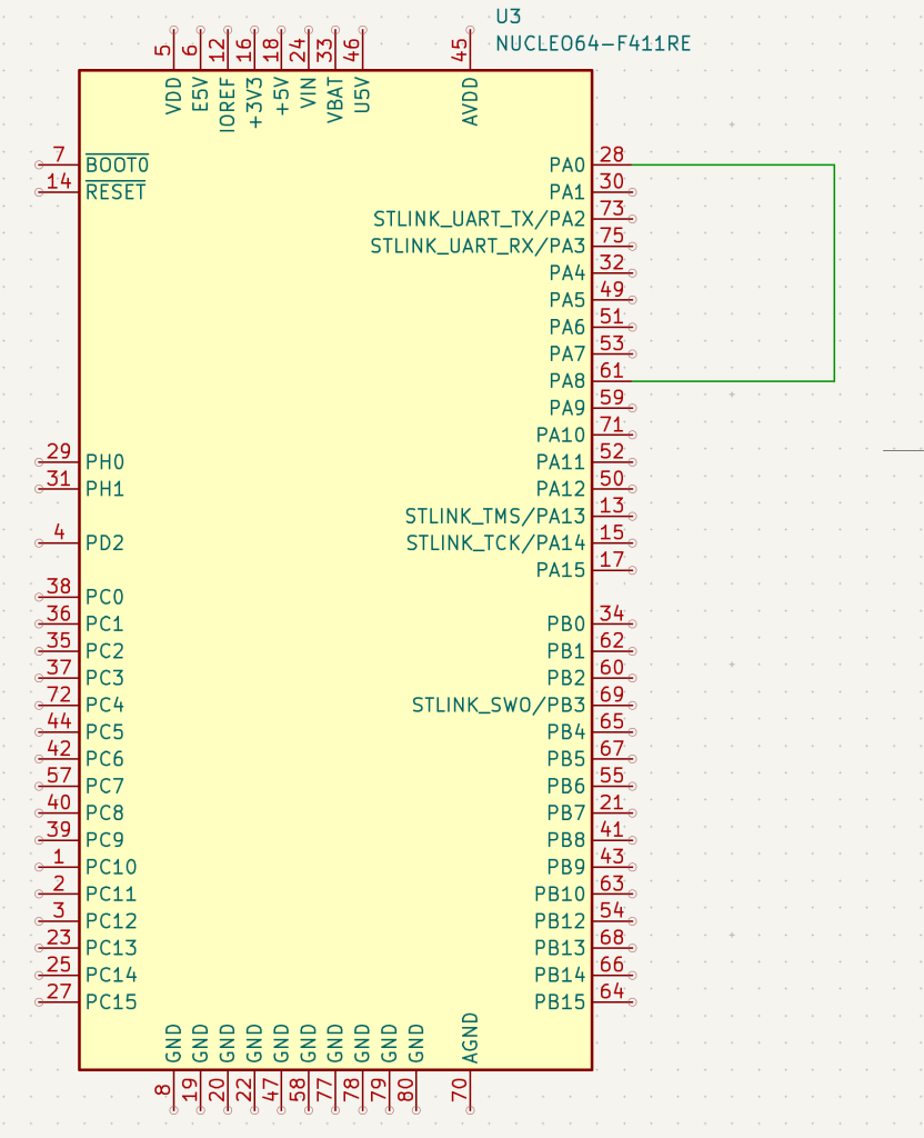
Simple, just connect a wire from PA8 to PA0.
5. Code:
You may download the code from here:
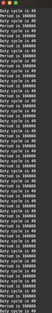
6. Results:
Since timer1 is configured with prescaler of 0 and ARR value of 600, this would give PWM signal with frequency of 166666Hz which is proven by measured value using PWM input:
Open serial terminal and set the baud to 115200 and you should get the following:
Happy coding 🙂
Add Comment