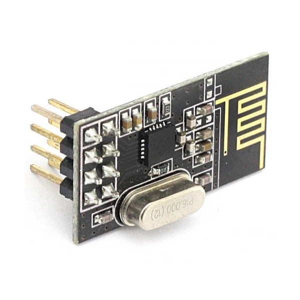
NRF24L01 is one of the legal RF communicators for modern applications. NRF24L01 is the cheapest one and it comes with great features. A single module communicates at 2.4 GHz frequency which makes it legal. It can transmit and receive data by a single module. Transreceiving is not its only ability, it can communicate with a total of 6 other same NRF24L01 modules at a single time. The device interfaces with the Arduino application and covers all kinds of remote-control applications. This wireless module uses SPI communication protocol and offers 10MBs data rate with 125 address range which makes it reliable the most reliable RF module. The RF module uses the GFSK module to transceiver the data.
In this guide, we shall cover the following:
- nRF24L01
- Connection with STM32.
- Configuring the required peripheral.
- Configuring nRF24L01.
1. nRF24L01:
In NRF24L01 there aren’t any special pins, all pins it offers to communicate are present in all microcontrollers and board. The device will interface with an external microcontroller/Arduino through these pins to operate. It consists of 8 pins. All available pins are:
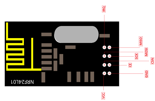
Power supply pins
VCC
The power pin of the module is VCC, which connects itself with the power supply.
GND
nRF24L01 operates with another microcontroller and it will need a common ground to operate with it. GND pin will solve the requirement of the common ground.
Communication Pins
CE
CE is an enable pin, which activates the transmission/receiving of the module. It will only activate the device when there is a HIGH state on itself.
CSN
This pin is for activating the data listening and processing from the microcontroller. To keep the data communication between the microcontroller and the module it should be HIGH.
SCK
It is the clock pulse pin of SPI communication in nRF24L01. The data will move between the module and the microcontroller according to the clock pulse on the SCK pin.
MOSI
The data transmitted from the microcontroller through SPI pins are going to receive by nRF24L01 at the MOSI pin.
MISO
The instructions transmitted from the nRF24L01 using SPI pins are going to receive by the microcontroller at the MISO pin.
IRQ Interrupt Pin
IRQ is an interrupt pin, which generates the event whenever a new data is available for SPI pins. It helps to send feedback to the transmitter.
NRF24L01 RF Module Feature
- It works at 2.4GHz frequency which makes it legal in almost every country.
- A single module can act as both a transmitter or receiver.
- A built-in antenna can send the data up to 100 meters.
- A module nRF24L01 can communicate with a maximum of 6 other modules at a time.
- It requires 3.3 volts to operate but voltages can only extend up to 3.6V otherwise it won’t take much time to heat up and burn.
- The device has a built-in oscillator of 16MHz.
- The transmission speed of nRF24L01 is 256kbps to 2Mbps.
- The device has 125 channel range which gives the feature of operating 125 different networks at a single place.
- The channel frequencies variate from 2400MHz to 2525MHz.
NRF24L01 Applications
- In the creation of a small mesh network, nRF24L01 is the best choice to use.
- Remote control applications at developing and commercial works wonderfully with nRF24L01.
- Most IoT applications at home level have this wireless module but at a small level only.
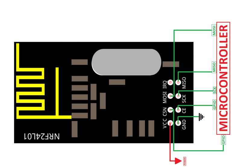
How to use the NRF24L01 Communication Module
nRF24L01 is usable with all the microcontrollers and smart boards but to use it, some pins and data information should be understood. To use the module connect it with another microcontroller with SPI protocol. First, give the power input to the devices and then attach their SPI pins according to the given circuit.
2. Connection with STM32:
In this guide, we need the following:
- 2x STM32F boards
- 2x LEDs
- 2x nRF24L01
- Hookup wires.
The connection shall be as following:
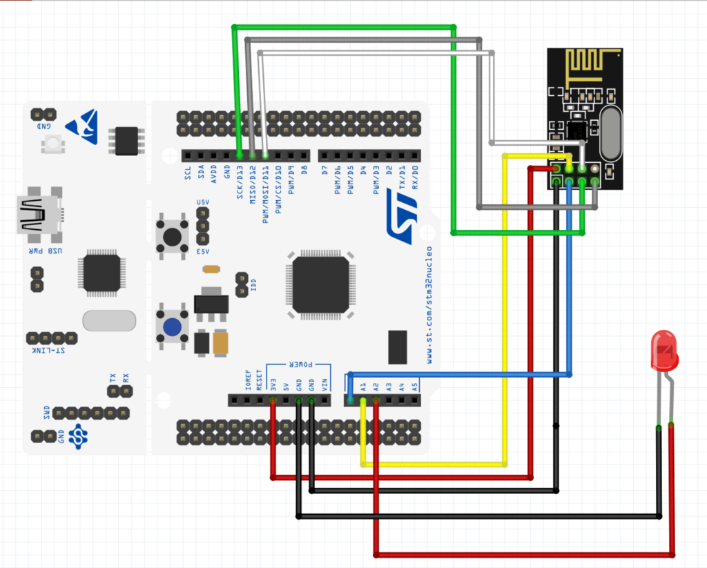
| STM32 | nRF24L01 |
| PA5 | SCK |
| PA6 | MISO |
| PA7 | MOSI |
| PA0 | nCS |
| PA1 | CE |
| PA4 | Anode of the LED |
3. Configuring the peripheral:
Since the module is using SPI, we shall use SPI1 of STM32F4 to communicate with the module.
We start off by configuring the SPI as following:
In spi.h file:
#ifndef SPI_H_
#define SPI_H_
#include "stdint.h"
void spi_init();
void spi1_transmit(uint8_t *data,uint32_t size);
void spi1_receive(uint8_t *data,uint32_t size);
#endif /* SPI_H_ */
for the spi.c source file:
#include "spi.h"
#include "stm32f4xx.h"

void spi_init()
	{

	#define AF05  (0x05)
	//enable clock for GPIOA
	RCC->AHB1ENR|=RCC_AHB1ENR_GPIOAEN;
	//set PA5, PA6 and PA7 to alternate function mode
	GPIOA->MODER|=GPIO_MODER_MODE5_1|GPIO_MODER_MODE6_1|GPIO_MODER_MODE7_1;
	//set which type of alternate function is
	GPIOA->AFR[0]|=(AF05<<20)|(AF05<<24)|(AF05<<28);
	//enable clock access to SPI1
	RCC->APB2ENR|=RCC_APB2ENR_SPI1EN;
	//set software slave managment
	SPI1->CR1|=SPI_CR1_SSM|SPI_CR1_SSI;
	//set SPI in master mode
	SPI1->CR1|=SPI_CR1_MSTR;
	//SPI1->CR1|=SPI_CR1_BR_0;
	SPI1->CR1|=SPI_CR1_SPE;
	}

void spi1_transmit(uint8_t *data,uint32_t size)
{
	uint32_t i=0;
	uint8_t temp;

	while(i<size)
	{
		/*Wait until TXE is set*/
		while(!(SPI1->SR & (SPI_SR_TXE))){}

		/*Write the data to the data register*/
		SPI1->DR = data[i];
		i++;
	}
	/*Wait until TXE is set*/
	while(!(SPI1->SR & (SPI_SR_TXE))){}

	/*Wait for BUSY flag to reset*/
	while((SPI1->SR & (SPI_SR_BSY))){}

	/*Clear OVR flag*/
	temp = SPI1->DR;
	temp = SPI1->SR;
}

void spi1_receive(uint8_t *data,uint32_t size)
{
	while(size)
	{
		/*Send dummy data*/
		SPI1->DR =0;

		/*Wait for RXNE flag to be set*/
		while(!(SPI1->SR & (SPI_SR_RXNE))){}

		/*Read data from data register*/
		*data++ = (SPI1->DR);
		size--;
	}
}
Since we are using LED for notification, we need to create two files, led.c and led.h
For the led.h:
#ifndef LED_H_
#define LED_H_

void led_init();
void led_off();
void toggle_led();


#endif /* LED_H_ */
For led.c
#include "led.h"
#include "stm32f4xx.h"

void led_init()
	{
	RCC->AHB1ENR|=RCC_AHB1ENR_GPIOAEN;
	GPIOA->MODER|=GPIO_MODER_MODE4_0;
	GPIOA->MODER&=~GPIO_MODER_MODE4_1;
	}

void led_on()
	{
	GPIOA->BSRR=GPIO_BSRR_BS4;
	}

void led_off()
	{
	GPIOA->BSRR=GPIO_BSRR_BR4;
	}

void toggle_led()
	{
	GPIOA->ODR^=GPIO_ODR_OD4;
	}
Also, we need to delay in milliseconds, in this case, we shall use systick to generate interrupt each 1 milliseconds as following:
For delay.h:
#ifndef DELAY_H_
#define DELAY_H_

#include "stdint.h"
void delay_init(uint32_t freq);
uint64_t millis();
void delay(uint32_t time);
#endif /* DELAY_H_ */
and delay.c
#include "delay.h"
#include "stm32f4xx.h"

#define	CTRL_ENABLE					(1U<<0)
#define CTRL_CLKSRC					(1U<<2)
#define CTRL_COUNTFLAG				(1U<<16)
#define CTRL_TICKINT				(1U<<1)


volatile uint64_t mil;

void delay_init(uint32_t freq){

	SysTick->LOAD  = (freq/1000) - 1;

	/*Clear systick current value register */
	SysTick->VAL = 0;

	/*Enable systick and select internal clk src*/
	SysTick->CTRL = CTRL_ENABLE | CTRL_CLKSRC ;

	/*Enable systick interrupt*/
	SysTick->CTRL  |= CTRL_TICKINT;

}


uint64_t millis()
	{
	__disable_irq();
	uint64_t ml=mil;
	__enable_irq();
	return ml;
	}


void delay(uint32_t time)
	{

	uint64_t start=millis();
	while((millis() - start) < time);

	}

void SysTick_Handler(void)
{
	mil++;
}
4. Configuring nRF24L01:
Before we start configuring the module, we need to create functions that allow us to perform the following:
- Chip select and chip enable
- Write to register.
- Multiple bytes write.
- Read a register.
- Read multiple bytes from a register.
- Write a command.
For those functions:
void CS_Select (void)
{
GPIOA->BSRR=GPIO_BSRR_BR1;
}

void CS_UnSelect (void)
{
GPIOA->BSRR=GPIO_BSRR_BS1;
}


void CE_Enable (void)
{
	GPIOA->BSRR=GPIO_BSRR_BS0;

}

void CE_Disable (void)
{
	GPIOA->BSRR=GPIO_BSRR_BR0;

}


// write a single byte to the particular register
void nrf24_WriteReg (uint8_t Reg, uint8_t Data)
{
	uint8_t buf[2];
	buf[0] = Reg|1<<5;
	buf[1] = Data;

	// Pull the CS Pin LOW to select the device
	CS_Select();

	spi1_transmit(buf, 2);

	// Pull the CS HIGH to release the device
	CS_UnSelect();
}

//write multiple bytes starting from a particular register
void nrf24_WriteRegMulti (uint8_t Reg, uint8_t *data, int size)
{
	uint8_t buf[2];
	buf[0] = Reg|1<<5;
//	buf[1] = Data;

	// Pull the CS Pin LOW to select the device
	CS_Select();

	spi1_transmit(buf,1);
	spi1_transmit(data, size);

	// Pull the CS HIGH to release the device
	CS_UnSelect();
}


uint8_t nrf24_ReadReg (uint8_t Reg)
{
	uint8_t data=0;

	// Pull the CS Pin LOW to select the device
	CS_Select();

	spi1_transmit(&Reg, 1);
	spi1_receive(&data,1);

	// Pull the CS HIGH to release the device
	CS_UnSelect();

	return data;
}


/* Read multiple bytes from the register */
void nrf24_ReadReg_Multi (uint8_t Reg, uint8_t *data, int size)
{
	// Pull the CS Pin LOW to select the device
	CS_Select();

	spi1_transmit(&Reg, 1);
	spi1_receive(data, size);
	// Pull the CS HIGH to release the device
	CS_UnSelect();
}


// send the command to the NRF
void nrfsendCmd (uint8_t cmd)
{
	// Pull the CS Pin LOW to select the device
	CS_Select();

	spi1_transmit( &cmd, 1);

	// Pull the CS HIGH to release the device
	CS_UnSelect();
}
Then we need to configure the CE and nCS as following:
void ncs_cs_init()
	{
  	/*enable clock access ti GPI)A*/
	RCC->AHB1ENR|=RCC_AHB1ENR_GPIOAEN;
  	/*Set PA0 and PA1 as output*/
	GPIOA->MODER|=GPIO_MODER_MODER0_0|GPIO_MODER_MODER1_0;
	GPIOA->MODER&=~(GPIO_MODER_MODER0_1|GPIO_MODER_MODER1_1);

	}
For initializing the nRF24L01:
void NRF24_Init (void)
{
	spi_init();
	ncs_cs_init();
	// disable the chip before configuring the device
	CE_Disable();


	// reset everything
	nrf24_reset (0);

	nrf24_WriteReg(CONFIG, 0);  // will be configured later

	nrf24_WriteReg(EN_AA, 0);  // No Auto ACK

	nrf24_WriteReg (EN_RXADDR, 0);  // Not Enabling any data pipe right now

	nrf24_WriteReg (SETUP_AW, 0x03);  // 5 Bytes for the TX/RX address

	nrf24_WriteReg (SETUP_RETR, 0);   // No retransmission

	nrf24_WriteReg (RF_CH, 0);  // will be setup during Tx or RX

	nrf24_WriteReg (RF_SETUP, 0x0E);   // Power= 0db, data rate = 2Mbps

	// Enable the chip after configuring the device
	CE_Enable();

}
For the header file:
#ifndef NRF_H_
#define NRF_H_

#include "stdint.h"

void NRF24_Init (void);

/* Memory Map */
#define CONFIG      0x00
#define EN_AA       0x01
#define EN_RXADDR   0x02
#define SETUP_AW    0x03
#define SETUP_RETR  0x04
#define RF_CH       0x05
#define RF_SETUP    0x06
#define STATUS      0x07
#define OBSERVE_TX  0x08
#define CD          0x09
#define RX_ADDR_P0  0x0A
#define RX_ADDR_P1  0x0B
#define RX_ADDR_P2  0x0C
#define RX_ADDR_P3  0x0D
#define RX_ADDR_P4  0x0E
#define RX_ADDR_P5  0x0F
#define TX_ADDR     0x10
#define RX_PW_P0    0x11
#define RX_PW_P1    0x12
#define RX_PW_P2    0x13
#define RX_PW_P3    0x14
#define RX_PW_P4    0x15
#define RX_PW_P5    0x16
#define FIFO_STATUS 0x17
#define DYNPD	    0x1C
#define FEATURE	    0x1D

/* Instruction Mnemonics */
#define R_REGISTER    0x00
#define W_REGISTER    0x20
#define REGISTER_MASK 0x1F
#define ACTIVATE      0x50
#define R_RX_PL_WID   0x60
#define R_RX_PAYLOAD  0x61
#define W_TX_PAYLOAD  0xA0
#define W_ACK_PAYLOAD 0xA8
#define FLUSH_TX      0xE1
#define FLUSH_RX      0xE2
#define REUSE_TX_PL   0xE3
#define NOP           0xFF


#endif /* NRF_H_ */
In part 2, we shall configure the module to transmit data
Happy coding 🙂
4 Comments
nrf24_reset – what should it content?
There is no reset pin on nRF24L01. You might have ESP8266 module.
Double check.
where is part 2?
Part 2:
https://blog.embeddedexpert.io/?p=878
Part 3:
https://blog.embeddedexpert.io/?p=886
Add Comment