In the past guides related to SPI, we worked only with single slave device. In this guide, we shall cover dealing with multiple slave devices. The slave devices in this case are:
- MPU9250.
- SSD1306 SPI OLED Monochrom display.
In this guide, we shall cover the following:
- SPI Configuration.
- MPU9250 and SSD1306 connection.
- MPU9250 and SSD1306 modification
- Code.
- Results.
1. SPI configuration:
To start off we shall create new header and source file with name of spi.h and spi.c respectively.
Within the header file:
Put the define guard as following:
#ifndef SPI_H_
#define SPI_H_


#endif /* SPI_H_ */
Within the guard, include stdint as following:
#include "stdint.h"
Since we are dealing with multiple slave devices, we shall use enum as following:
typedef enum
{

	MPU9250_CS=0,
	SSD1306_CS=1


}SlaveSelectTypedef;
This can be passed as argument to slave select and deselect functions.
Now, declare the following functions:
void Slave_Pins_init();

void SPI_Pins_Init();

void SPI_Configure();

void SPI_Write(uint8_t *data,uint32_t size);

void SPI_Receive(uint8_t *data,uint32_t size);

void Slave_Select(SlaveSelectTypedef slave);

void Slave_Deselect(SlaveSelectTypedef slave);
These are the function to be implemented within the source file.
Hence, the entire header file as following:
#ifndef SPI_H_
#define SPI_H_

#include "stdint.h"

typedef enum
{

	MPU9250_CS=0,
	SSD1306_CS=1


}SlaveSelectTypedef;


void Slave_Pins_init();

void SPI_Pins_Init();

void SPI_Configure();

void SPI_Write(uint8_t *data,uint32_t size);

void SPI_Receive(uint8_t *data,uint32_t size);

void Slave_Select(SlaveSelectTypedef slave);

void Slave_Deselect(SlaveSelectTypedef slave);

#endif /* SPI_H_ */
Moving on to the source file.
We start off by including spi.h and stm32f4xx.h header file as following:
#include "spi.h"

#include "stm32f4xx.h"
For information about which pins and how configure SPI, check this guide from here.
For SPI pins initialization:
void SPI_Pins_Init()
{
	RCC->AHB1ENR|=RCC_AHB1ENR_GPIOAEN; //enable clock for GPIOA

	//set PA5, PA6 and PA7 to alternate function mode
	GPIOA->MODER|=GPIO_MODER_MODE5_1|GPIO_MODER_MODE6_1|GPIO_MODER_MODE7_1;
	GPIOA->MODER &=~(GPIO_MODER_MODE5_0|GPIO_MODER_MODE6_0|GPIO_MODER_MODE7_0);


	/*select which AF for PA5, PA6 and PA7 which is AF05*/
	GPIOA->AFR[0]|=(0x05<<20)|(0x05<<24)|(0x05<<28);
}
Salve pins initialization:
void Slave_Pins_init()
{
	/*Enable clock access to GPIOA*/
	RCC->AHB1ENR|=RCC_AHB1ENR_GPIOAEN;

	/*Set PA0 and PA1 to output mode*/
	GPIOA->MODER|=GPIO_MODER_MODE0_0|GPIO_MODER_MODE1_0;

	GPIOA->MODER&=~(GPIO_MODER_MODE0_1|GPIO_MODER_MODE1_1);

	/*Set PA0 to PA1 to high state*/
	GPIOA->BSRR=GPIO_BSRR_BS0|GPIO_BSRR_BS1;
}
SPI configuration:
void SPI_Configure()
{
	/*Enable clock access to SPI1 module*/
	RCC->APB2ENR |= RCC_APB2ENR_SPI1EN;

	/*Set clock to fPCLK/2*/
	SPI1->CR1 &=~(1U<<3);
	SPI1->CR1 &=~(1U<<4);
	SPI1->CR1 &=~(1U<<5);

	/*Enable full duplex*/
	SPI1->CR1 &=~(1U<<10);

	/*Set MSB first*/
	SPI1->CR1 &= ~(1U<<7);

	/*Set mode to MASTER*/
	SPI1->CR1 |= (1U<<2);

	/*Set 8 bit data mode*/
	SPI1->CR1 &= ~(1U<<11);

	/*Select software slave management by
	 * setting SSM=1 and SSI=1*/
	SPI1->CR1 |= (1<<8);
	SPI1->CR1 |= (1<<9);

	/*Enable SPI module*/
	SPI1->CR1 |= (1<<6);
}
SPI write:
void SPI_Write(uint8_t *data,uint32_t size)
{
	uint32_t i=0;

	while(i<size)
	{
		/*Wait until TXE is set*/
		while(!(SPI1->SR & (SPI_SR_TXE))){}

		/*Write the data to the data register*/
		SPI1->DR =(uint8_t) data[i];
		i++;
	}
	/*Wait until TXE is set*/
	while(!(SPI1->SR & (SPI_SR_TXE))){}

	/*Wait for BUSY flag to reset*/
	while((SPI1->SR & (SPI_SR_BSY))){}

	/*Clear OVR flag*/
	(void)SPI1->DR;
	(void)SPI1->SR;
}
SPI Read:
void SPI_Receive(uint8_t *data,uint32_t size)
{

	while(size)
	{
		/*Send dummy data*/
		SPI1->DR =0xFF;

		/*Wait for RXNE flag to be set*/
		while(!(SPI1->SR & (SPI_SR_RXNE))){}

		/*Read data from data register*/
		*data++ = (SPI1->DR);
		size--;
	}
}
Now for slave select and deselect.
Since we already created enums for the salves devices, we shall pass this enum as argument to both select and deselect functions.
For select function:
void Slave_Select(SlaveSelectTypedef slave)
Using switch state, we can select the slave as following:
	switch (slave)
	{
		case MPU9250_CS: GPIOA->BSRR=GPIO_BSRR_BR0; break;

		case SSD1306_CS: GPIOA->BSRR=GPIO_BSRR_BR1; break;

		default: break;
Since selecting slave requires setting the pin to low, we can use BSRR register of the GPIO to achieve this.
Also, for deselecting the slave, the pin should be pulled high as following:
void Slave_Deselect(SlaveSelectTypedef slave)
{
	switch (slave)
	{
		case MPU9250_CS: GPIOA->BSRR=GPIO_BSRR_BS0; break;

		case SSD1306_CS: GPIOA->BSRR=GPIO_BSRR_BS1; break;

		default: break;
	}
}
Hence, the source file as following:
#include "spi.h"

#include "stm32f4xx.h"


void SPI_Pins_Init()
{
	RCC->AHB1ENR|=RCC_AHB1ENR_GPIOAEN; //enable clock for GPIOA

	//set PA5, PA6 and PA7 to alternate function mode
	GPIOA->MODER|=GPIO_MODER_MODE5_1|GPIO_MODER_MODE6_1|GPIO_MODER_MODE7_1;
	GPIOA->MODER &=~(GPIO_MODER_MODE5_0|GPIO_MODER_MODE6_0|GPIO_MODER_MODE7_0);


	/*select which AF for PA5, PA6 and PA7 which is AF05*/
	GPIOA->AFR[0]|=(0x05<<20)|(0x05<<24)|(0x05<<28);
}


void Slave_Pins_init()
{
	/*Enable clock access to GPIOA*/
	RCC->AHB1ENR|=RCC_AHB1ENR_GPIOAEN;

	/*Set PA0 and PA1 to output mode*/
	GPIOA->MODER|=GPIO_MODER_MODE0_0|GPIO_MODER_MODE1_0;

	GPIOA->MODER&=~(GPIO_MODER_MODE0_1|GPIO_MODER_MODE1_1);

	/*Set PA0 to PA1 to high state*/
	GPIOA->BSRR=GPIO_BSRR_BS0|GPIO_BSRR_BS1;
}

void SPI_Configure()
{
	/*Enable clock access to SPI1 module*/
	RCC->APB2ENR |= RCC_APB2ENR_SPI1EN;

	/*Set clock to fPCLK/2*/
	SPI1->CR1 &=~(1U<<3);
	SPI1->CR1 &=~(1U<<4);
	SPI1->CR1 &=~(1U<<5);

	/*Enable full duplex*/
	SPI1->CR1 &=~(1U<<10);

	/*Set MSB first*/
	SPI1->CR1 &= ~(1U<<7);

	/*Set mode to MASTER*/
	SPI1->CR1 |= (1U<<2);

	/*Set 8 bit data mode*/
	SPI1->CR1 &= ~(1U<<11);

	/*Select software slave management by
	 * setting SSM=1 and SSI=1*/
	SPI1->CR1 |= (1<<8);
	SPI1->CR1 |= (1<<9);

	/*Enable SPI module*/
	SPI1->CR1 |= (1<<6);
}

void SPI_Write(uint8_t *data,uint32_t size)
{
	uint32_t i=0;

	while(i<size)
	{
		/*Wait until TXE is set*/
		while(!(SPI1->SR & (SPI_SR_TXE))){}

		/*Write the data to the data register*/
		SPI1->DR =(uint8_t) data[i];
		i++;
	}
	/*Wait until TXE is set*/
	while(!(SPI1->SR & (SPI_SR_TXE))){}

	/*Wait for BUSY flag to reset*/
	while((SPI1->SR & (SPI_SR_BSY))){}

	/*Clear OVR flag*/
	(void)SPI1->DR;
	(void)SPI1->SR;
}


void SPI_Receive(uint8_t *data,uint32_t size)
{

	while(size)
	{
		/*Send dummy data*/
		SPI1->DR =0xFF;

		/*Wait for RXNE flag to be set*/
		while(!(SPI1->SR & (SPI_SR_RXNE))){}

		/*Read data from data register*/
		*data++ = (SPI1->DR);
		size--;
	}
}


void Slave_Select(SlaveSelectTypedef slave)
{
	switch (slave)
	{
		case MPU9250_CS: GPIOA->BSRR=GPIO_BSRR_BR0; break;

		case SSD1306_CS: GPIOA->BSRR=GPIO_BSRR_BR1; break;

		default: break;
	}
}

void Slave_Deselect(SlaveSelectTypedef slave)
{
	switch (slave)
	{
		case MPU9250_CS: GPIOA->BSRR=GPIO_BSRR_BS0; break;

		case SSD1306_CS: GPIOA->BSRR=GPIO_BSRR_BS1; break;

		default: break;
	}
}
Thats all for the SPI driver development.
2. MPU9259 and SSD1306 connection:
The connection of the two slave devices as following:
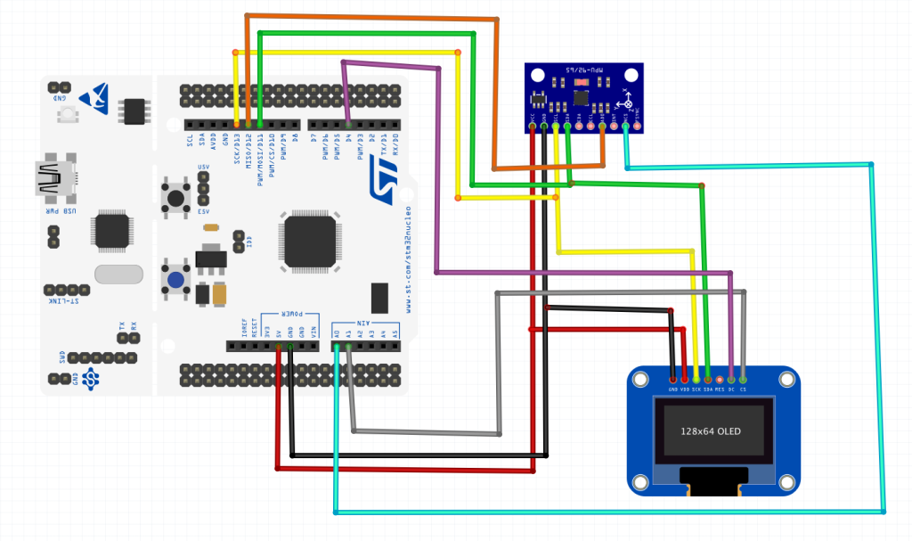
| STM32F411 Nucleo | SSD1306 SPI OLED | MPU9250 |
| 5V | Vcc | Vcc |
| GND | GND | GND |
| SCK (PA5) | SCL | SCK |
| MOSI (PA7) | SDA | SDA |
| MISO | – | ADO |
| PA0 | CSN | – |
| PA1 | – | CS |
| PA10 | DC | – |
3. MPU9250 and SSD1306 modification:
The modification for SSD1306 SPI for write data, command and multidata as following:
void SSD1306_WRITECOMMAND(uint8_t command)
{
	OLED_CommMode();
	Slave_Select(SSD1306_CS);
	SPI_Write(&command,1);
	Slave_Deselect(SSD1306_CS);
}

void SSD1306_WRITEDATA(uint8_t command)
{
	OLED_DataMode();
	Slave_Select(SSD1306_CS);
	SPI_Write(&command,1);
	Slave_Deselect(SSD1306_CS);
}

void SSD1306_Write_Multi_Data(uint8_t * data, uint16_t length)
{
	OLED_DataMode();
	Slave_Select(SSD1306_CS);
	SPI_Write(data,length);
	Slave_Deselect(SSD1306_CS);

}
For SSD1306 SPI OLED code, from here.
For full MPU code, please refer to the following guide here.
The modification as following for writing process:
	Slave_Select(MPU9250_CS);
	SPI_Write(data,2);
	Slave_Deselect(MPU9250_CS);
For reading process:
	Slave_Select(MPU9250_CS);
	SPI_Write(data,1);
	SPI_Receive((uint8_t*)(accelBuf),6);
	Slave_Deselect(MPU9250_CS);
The rest of the code will remain the same.
4. Code:
You may download the entire source code from here:
5. Results:
For testing functionality of both MPU9250 and SSD1306, the following is the implementation of main.c:
#include "delay.h"
#include "oled.h"
#include "MPU9250.h"
#include "spi.h"
#include "stdio.h"

char zz[30];


extern void uart2_rxtx_init(void);


float ax,ay,az;
uint16_t count;
int main(void)
{

	uart2_rxtx_init();
	SPI_Pins_Init();
	Slave_Pins_init();
	SPI_Configure();
	SSD1306_Init();
	MPU9250_beginAccel(ACC_FULL_SCALE_2_G);


	while(1)
	{
		MPU9250_accelUpdate();

		ax=MPU9250_accelX();
		ay=MPU9250_accelY();
		az=MPU9250_accelZ();

		sprintf(zz,"ax=%0.2f",MPU9250_accelX());
		SSD1306_GotoXY (0,0);
		SSD1306_Puts (zz, &Font_7x10, 1);

		sprintf(zz,"ay=%0.2f",MPU9250_accelY());
		SSD1306_GotoXY (0,10);
		SSD1306_Puts (zz, &Font_7x10, 1);

		sprintf(zz,"az=%0.2f",MPU9250_accelZ());
		SSD1306_GotoXY (0,20);
		SSD1306_Puts (zz, &Font_7x10, 1);


		SSD1306_GotoXY (0,30);
		sprintf(zz,"%d",count++);
		SSD1306_Puts (zz, &Font_7x10, 1);

		SSD1306_UpdateScreen();

		delay(30);

	}

}
The results as following:
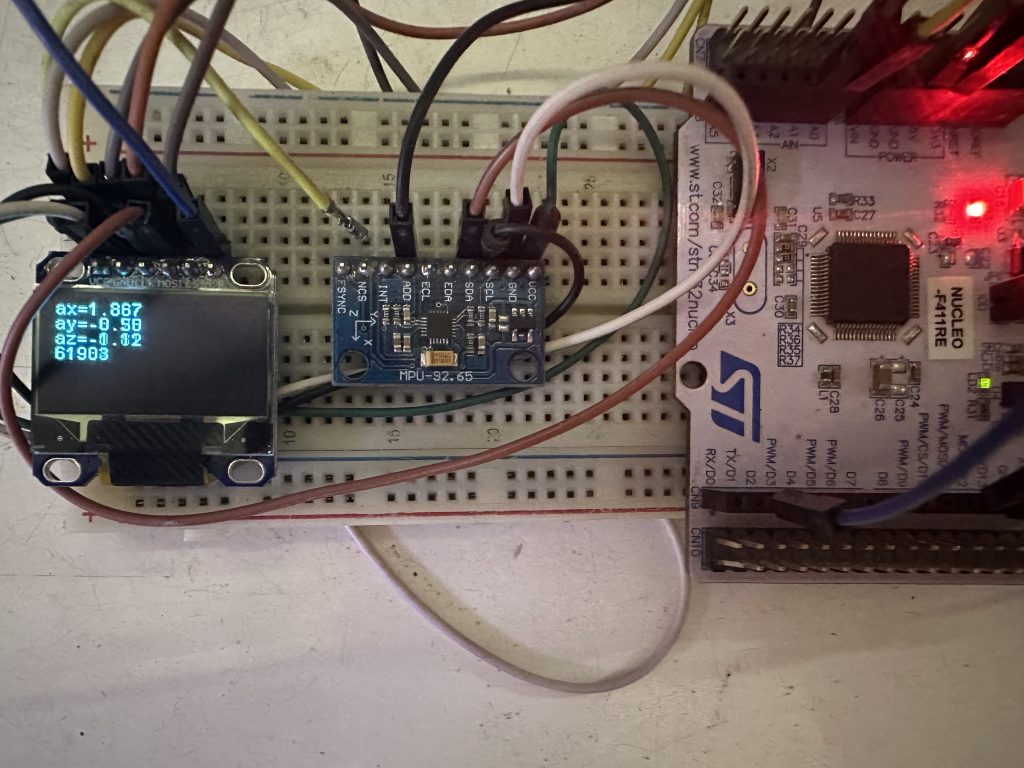
Both MPU9250 and SSD1306 are working.
Happy coding 🙂
3 Comments
Nice tutorial, thanks for the blog post. Which MCU is used for this tutorial?
Hi,
STM32F411-Nucleo64 is being used in this guide.
Alright, thanks.
Add Comment