
In the previous guide of PWM (here), we saw how to configure the timer to operate in PWM mode and update the duty cycle using for loop.
In this guide, we shall use DMA and set of predefined duty cycle to update two channels of PWM.
In this guide, we shall cover the following:
- GPIO configuration.
- Timer configuration
- DMA configuration.
- Code.
- Results.
1. GPIO configuration
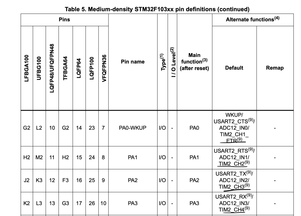
From the previous guide, we know that PA0, PA1, PA2 and PA3 are for TIM2_CH1, TIM2_CH2, TIM2_CH3 and TIM2_CH4 respectively:
Hence, we shall configure both pins as alternate output push-pull configuration and output speed to maximum of 50MHz as following:
	RCC->APB2ENR|=RCC_APB2ENR_IOPAEN;

	/*Configure PA0 as Output Alternate Push/Pull */
	GPIOA->CRL|=GPIO_CRL_MODE0;
	GPIOA->CRL|=(GPIO_CRL_CNF0_1);
	GPIOA->CRL&=~(GPIO_CRL_CNF0_0);

	/*Configure PA1 as Output Alternate Push/Pull */
	GPIOA->CRL|=GPIO_CRL_MODE1;
	GPIOA->CRL|=(GPIO_CRL_CNF1_1);
	GPIOA->CRL&=~(GPIO_CRL_CNF1_0);
Also, we shall not remap the pins of TIM2:
	/*Don't remap the pin*/
	AFIO->MAPR&=~AFIO_MAPR_TIM2_REMAP;
Thats all for GPIO configuration.
2. Timer configuration:
First enable clock access to TIM2 as following:
	/*Enable clock access to timer2*/
	RCC->APB1ENR|=RCC_APB1ENR_TIM2EN;
Set the prescaler and ARR to be 0 and 1600 respectively:
	TIM2->PSC=0;
	TIM2->ARR=1600;
Set both pins as PWM using OC1M and OC2M configuration:
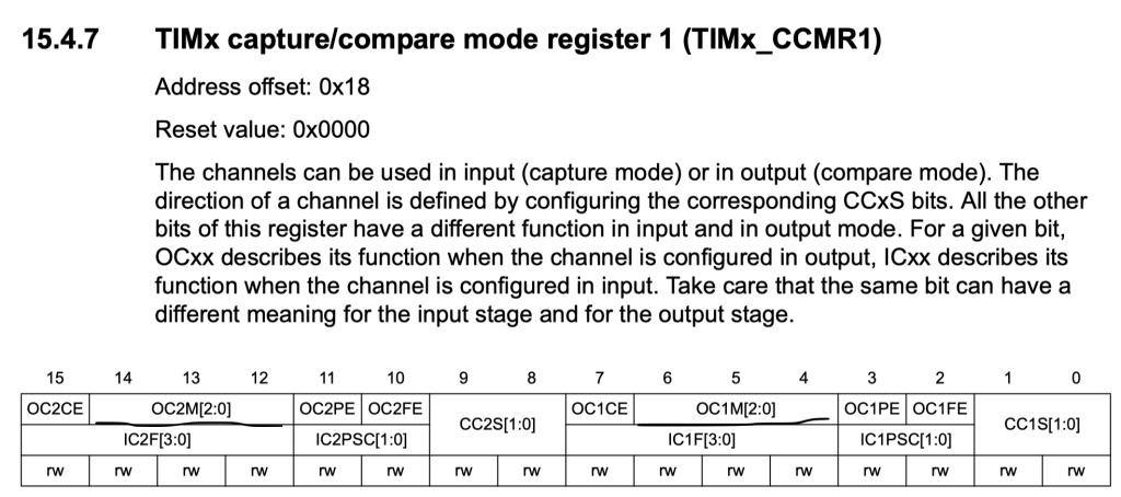
TIM2->CCMR1|=TIM_CCMR1_OC1M_2|TIM_CCMR1_OC1M_1|TIM_CCMR1_OC2M_2|TIM_CCMR1_OC2M_1;
Enable both channel:
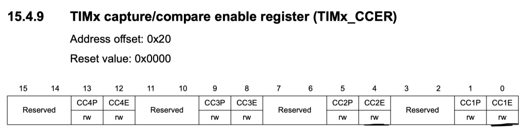
TIM2->CCER|=TIM_CCER_CC1E|TIM_CCER_CC2E;
Set the timer to trigger DMA request each Capture/Compare is happened.
To do such thing, CC1DE and CC2DE bit should be set in DIER register:
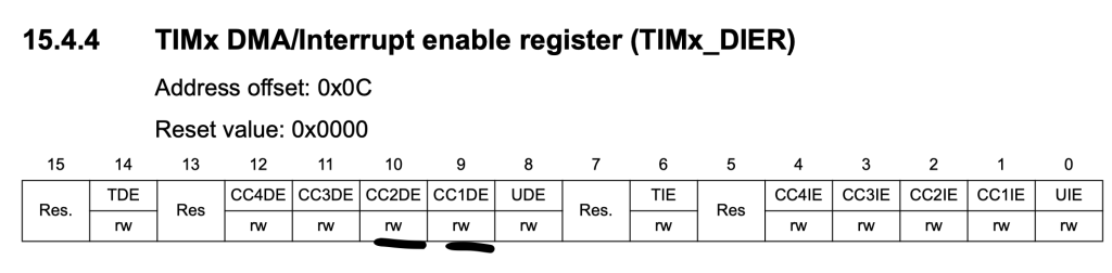
TIM2->DIER|=TIM_DIER_CC1DE|TIM_DIER_CC2DE;
Note: DON’T ENABLE THE TIMER YET.
3. DMA Configuration:
Since STM32F103 has only 1 DMA, we shall enable clock access to it as following:
Since the DMA is connected to AHB bus, we can enable clock access to it as following:
RCC->AHBENR|=RCC_AHBENR_DMA1EN;
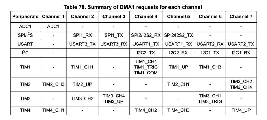
Then we need to know which DMA channels are responsible for TIM2_CH1 and TIM2_CH2.
From the reference manual, DMA request table, we can find that DMA1_Stream5 and DMA1_Stream7 are responsible for TIM2_CH1 and TIM2_CH2 respectively:
Hence, we shall configure both channels with the following parameters:
- Memory and peripheral size to 16-bit (half word).
- Memory increment mode.
- DMA in circular mode.
- Direction is read from memory.
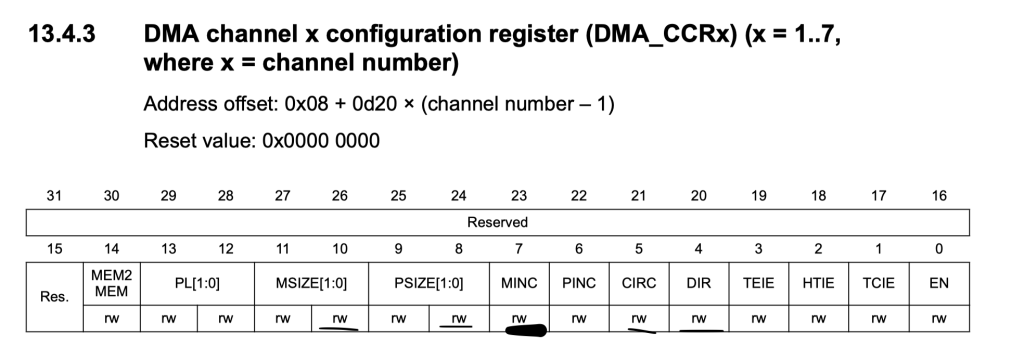
DMA1_Channel5->CCR=DMA_CCR_MSIZE_0|DMA_CCR_PSIZE_0|
			DMA_CCR_MINC|DMA_CCR_CIRC|DMA_CCR_DIR;
DMA1_Channel7->CCR=DMA_CCR_MSIZE_0|DMA_CCR_PSIZE_0|
			DMA_CCR_MINC|DMA_CCR_CIRC|DMA_CCR_DIR;
Note: DON’T ENABLE THE CHANNELs YET.
Set the memory address to the array that holds the duty cycle values:
#define sample_size		200


uint16_t lookUp1[sample_size] = {0,50 ,100 ,151 ,201 ,250 ,300 ,349 ,398 ,446 ,494 ,542 ,589 ,635 ,681
	,726 ,771 ,814 ,857 ,899 ,940 ,981 ,1020 ,1058 ,1095 ,1131 ,1166 ,1200 ,1233 ,1264
	,1294 ,1323 ,1351 ,1377 ,1402 ,1426 ,1448 ,1468 ,1488 ,1505 ,1522 ,1536 ,1550 ,1561
	,1572 ,1580 ,1587 ,1593 ,1597 ,1599 ,1600 ,1599 ,1597 ,1593 ,1587 ,1580 ,1572 ,1561
	,1550 ,1536 ,1522 ,1505 ,1488 ,1468 ,1448 ,1426 ,1402 ,1377 ,1351 ,1323 ,1294 ,1264
	,1233 ,1200 ,1166 ,1131 ,1095 ,1058 ,1020 ,981 ,940 ,899 ,857 ,814 ,771 ,726 ,681 ,635
	,589 ,542 ,494 ,446 ,398 ,349 ,300 ,250 ,201 ,151 ,100 ,50,0 ,0 ,0 ,0 ,0 ,0 ,0 ,0 ,0 ,0
	,0 ,0 ,0 ,0 ,0 ,0 ,0 ,0 ,0 ,0 ,0 ,0 ,0 ,0 ,0 ,0 ,0 ,0 ,0 ,0 ,0 ,0 ,0 ,0 ,0 ,0 ,0 ,0 ,0 ,0
	,0 ,0 ,0 ,0 ,0 ,0 ,0 ,0 ,0 ,0 ,0 ,0 ,0 ,0 ,0 ,0 ,0 ,0 ,0 ,0 ,0 ,0 ,0 ,0 ,0 ,0 ,0 ,0 ,0 ,0
	,0 ,0 ,0 ,0 ,0 ,0 ,0 ,0 ,0 ,0 ,0 ,0 ,0 ,0 ,0 ,0 ,0 ,0 ,0 ,0 ,0 ,0 ,0 ,0 ,0 ,0 ,0 ,0 ,0 ,0 };

uint16_t lookUp2[sample_size] = {0 ,0 ,0 ,0 ,0 ,0 ,0 ,0 ,0 ,0 ,0 ,0 ,0 ,0 ,0 ,0 ,0 ,0 ,0 ,0 ,0 ,0 ,0 ,0 ,0
	,0 ,0 ,0 ,0 ,0 ,0 ,0 ,0 ,0 ,0 ,0 ,0 ,0 ,0 ,0 ,0 ,0 ,0 ,0 ,0 ,0 ,0 ,0 ,0 ,0 ,0 ,0 ,0 ,0 ,0
	,0 ,0 ,0 ,0 ,0 ,0 ,0 ,0 ,0 ,0 ,0 ,0 ,0 ,0 ,0 ,0 ,0 ,0 ,0 ,0 ,0 ,0 ,0 ,0 ,0 ,0 ,0 ,0 ,0 ,0
	,0 ,0 ,0 ,0 ,0 ,0 ,0 ,0 ,0 ,0 ,0 ,0 ,0 ,0 ,0 ,50 ,100 ,151 ,201 ,250 ,300 ,349 ,398 ,446 ,494
	,542 ,589 ,635 ,681 ,726 ,771 ,814 ,857 ,899 ,940 ,981 ,1020 ,1058 ,1095 ,1131 ,1166 ,1200 ,1233
	,1264 ,1294 ,1323 ,1351 ,1377 ,1402 ,1426 ,1448 ,1468 ,1488 ,1505 ,1522 ,1536 ,1550 ,1561 ,1572 ,1580
	,1587 ,1593 ,1597 ,1599 ,1600 ,1599 ,1597 ,1593 ,1587 ,1580 ,1572 ,1561 ,1550 ,1536 ,1522 ,1505 ,1488
	,1468 ,1448 ,1426 ,1402 ,1377 ,1351 ,1323 ,1294 ,1264 ,1233 ,1200 ,1166 ,1131 ,1095 ,1058 ,1020 ,981
	,940 ,899 ,857 ,814 ,771 ,726 ,681 ,635 ,589 ,542 ,494 ,446 ,398 ,349 ,300 ,250 ,201 ,151 ,100 ,50 ,0};
DMA1_Channel5->CMAR=(uint32_t)lookUp1;
DMA1_Channel7->CMAR=(uint32_t)lookUp2;
Set number of transfers to be 200 (size of the array):
DMA1_Channel5->CNDTR=(uint16_t)sample_size;
DMA1_Channel7->CNDTR=(uint16_t)sample_size;
Set the peripheral address to CCR1 and CCR2 respectively:
DMA1_Channel5->CPAR=(uint32_t)(&TIM2->CCR1);
DMA1_Channel7->CPAR=(uint32_t)(&TIM2->CCR2);
Enable both channels:
	DMA1_Channel5->CCR|=DMA_CCR_EN;
	DMA1_Channel7->CCR|=DMA_CCR_EN;
Finally, enable the timer:
TIM2->CR1|=TIM_CR1_CEN;
4. Code:
The entire code as following:
#include "stm32f1xx.h"

/*DMA1 Channels
 *
 * Channel5 for TIM2_CH1
 * Channel7 for TIM2_CH2
 *
 * */

#define sample_size		200


uint16_t lookUp1[sample_size] = {0,50 ,100 ,151 ,201 ,250 ,300 ,349 ,398 ,446 ,494 ,542 ,589 ,635 ,681
	,726 ,771 ,814 ,857 ,899 ,940 ,981 ,1020 ,1058 ,1095 ,1131 ,1166 ,1200 ,1233 ,1264
	,1294 ,1323 ,1351 ,1377 ,1402 ,1426 ,1448 ,1468 ,1488 ,1505 ,1522 ,1536 ,1550 ,1561
	,1572 ,1580 ,1587 ,1593 ,1597 ,1599 ,1600 ,1599 ,1597 ,1593 ,1587 ,1580 ,1572 ,1561
	,1550 ,1536 ,1522 ,1505 ,1488 ,1468 ,1448 ,1426 ,1402 ,1377 ,1351 ,1323 ,1294 ,1264
	,1233 ,1200 ,1166 ,1131 ,1095 ,1058 ,1020 ,981 ,940 ,899 ,857 ,814 ,771 ,726 ,681 ,635
	,589 ,542 ,494 ,446 ,398 ,349 ,300 ,250 ,201 ,151 ,100 ,50,0 ,0 ,0 ,0 ,0 ,0 ,0 ,0 ,0 ,0
	,0 ,0 ,0 ,0 ,0 ,0 ,0 ,0 ,0 ,0 ,0 ,0 ,0 ,0 ,0 ,0 ,0 ,0 ,0 ,0 ,0 ,0 ,0 ,0 ,0 ,0 ,0 ,0 ,0 ,0
	,0 ,0 ,0 ,0 ,0 ,0 ,0 ,0 ,0 ,0 ,0 ,0 ,0 ,0 ,0 ,0 ,0 ,0 ,0 ,0 ,0 ,0 ,0 ,0 ,0 ,0 ,0 ,0 ,0 ,0
	,0 ,0 ,0 ,0 ,0 ,0 ,0 ,0 ,0 ,0 ,0 ,0 ,0 ,0 ,0 ,0 ,0 ,0 ,0 ,0 ,0 ,0 ,0 ,0 ,0 ,0 ,0 ,0 ,0 ,0 };

uint16_t lookUp2[sample_size] = {0 ,0 ,0 ,0 ,0 ,0 ,0 ,0 ,0 ,0 ,0 ,0 ,0 ,0 ,0 ,0 ,0 ,0 ,0 ,0 ,0 ,0 ,0 ,0 ,0
	,0 ,0 ,0 ,0 ,0 ,0 ,0 ,0 ,0 ,0 ,0 ,0 ,0 ,0 ,0 ,0 ,0 ,0 ,0 ,0 ,0 ,0 ,0 ,0 ,0 ,0 ,0 ,0 ,0 ,0
	,0 ,0 ,0 ,0 ,0 ,0 ,0 ,0 ,0 ,0 ,0 ,0 ,0 ,0 ,0 ,0 ,0 ,0 ,0 ,0 ,0 ,0 ,0 ,0 ,0 ,0 ,0 ,0 ,0 ,0
	,0 ,0 ,0 ,0 ,0 ,0 ,0 ,0 ,0 ,0 ,0 ,0 ,0 ,0 ,0 ,50 ,100 ,151 ,201 ,250 ,300 ,349 ,398 ,446 ,494
	,542 ,589 ,635 ,681 ,726 ,771 ,814 ,857 ,899 ,940 ,981 ,1020 ,1058 ,1095 ,1131 ,1166 ,1200 ,1233
	,1264 ,1294 ,1323 ,1351 ,1377 ,1402 ,1426 ,1448 ,1468 ,1488 ,1505 ,1522 ,1536 ,1550 ,1561 ,1572 ,1580
	,1587 ,1593 ,1597 ,1599 ,1600 ,1599 ,1597 ,1593 ,1587 ,1580 ,1572 ,1561 ,1550 ,1536 ,1522 ,1505 ,1488
	,1468 ,1448 ,1426 ,1402 ,1377 ,1351 ,1323 ,1294 ,1264 ,1233 ,1200 ,1166 ,1131 ,1095 ,1058 ,1020 ,981
	,940 ,899 ,857 ,814 ,771 ,726 ,681 ,635 ,589 ,542 ,494 ,446 ,398 ,349 ,300 ,250 ,201 ,151 ,100 ,50 ,0};


int main(void)
{
	RCC->APB2ENR|=RCC_APB2ENR_IOPAEN;

	/*Configure PA0 as Output Alternate Push/Pull */
	GPIOA->CRL|=GPIO_CRL_MODE0;
	GPIOA->CRL|=(GPIO_CRL_CNF0_1);
	GPIOA->CRL&=~(GPIO_CRL_CNF0_0);

	/*Configure PA1 as Output Alternate Push/Pull */
	GPIOA->CRL|=GPIO_CRL_MODE1;
	GPIOA->CRL|=(GPIO_CRL_CNF1_1);
	GPIOA->CRL&=~(GPIO_CRL_CNF1_0);

	/*Don't remap the pin*/
	AFIO->MAPR&=~AFIO_MAPR_TIM2_REMAP;


	/*Enable clock access to timer2*/
	RCC->APB1ENR|=RCC_APB1ENR_TIM2EN;

	/*Configure timer2*/
	TIM2->PSC=0;
	TIM2->ARR=1600;
	TIM2->CCMR1|=TIM_CCMR1_OC1M_2|TIM_CCMR1_OC1M_1|TIM_CCMR1_OC2M_2|TIM_CCMR1_OC2M_1;
	TIM2->CCER|=TIM_CCER_CC1E|TIM_CCER_CC2E;

	TIM2->DIER|=TIM_DIER_CC1DE|TIM_DIER_CC2DE;


	/*DMA configuration*/

	RCC->AHBENR|=RCC_AHBENR_DMA1EN;

	DMA1_Channel5->CCR=DMA_CCR_MSIZE_0|DMA_CCR_PSIZE_0|
			DMA_CCR_MINC|DMA_CCR_CIRC|DMA_CCR_DIR;

	DMA1_Channel5->CNDTR=(uint16_t)sample_size;
	DMA1_Channel5->CMAR=(uint32_t)lookUp1;
	DMA1_Channel5->CPAR=(uint32_t)(&TIM2->CCR1);

	DMA1_Channel7->CCR=DMA_CCR_MSIZE_0|DMA_CCR_PSIZE_0|
			DMA_CCR_MINC|DMA_CCR_CIRC|DMA_CCR_DIR;

	DMA1_Channel7->CNDTR=(uint16_t)sample_size;
	DMA1_Channel7->CMAR=(uint32_t)lookUp2;
	DMA1_Channel7->CPAR=(uint32_t)(&TIM2->CCR2);

	DMA1_Channel5->CCR|=DMA_CCR_EN;
	DMA1_Channel7->CCR|=DMA_CCR_EN;

	TIM2->CR1|=TIM_CR1_CEN;

	while(1)
	{


	}
}
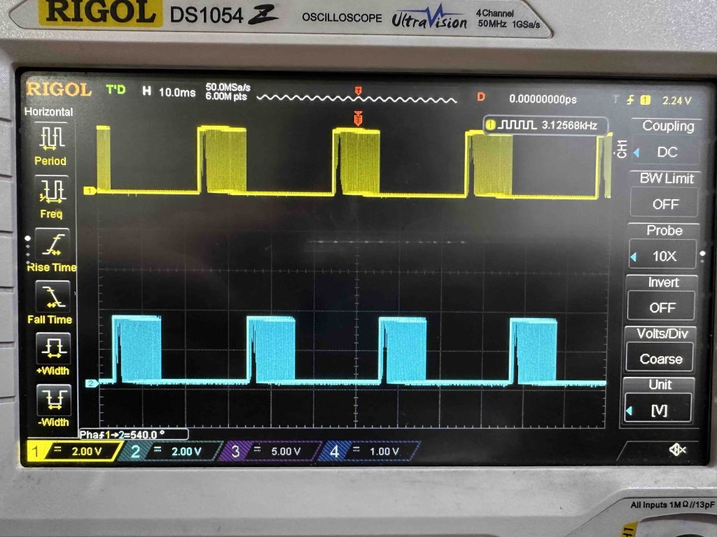
5. Results:
Probe both PA0 and PA1 using oscilloscope, you should get the following:
Happy coding 🙂
8 Comments
The reason this program does not work properly is that capture registers are not buffered. By enabling preload of CCR1 and CCR2, the program functions properly.
Change the code to read like this:
/*Set pins as PWM using OC1M and OC2M*/ /*and enable preload*/
TIM2->CCMR1|=TIM_CCMR1_OC1M_2|TIM_CCMR1_OC1M_1|TIM_CCMR1_OC2M_2|
TIM_CCMR1_OC2M_1|TIM_CCMR1_OC2PE|TIM_CCMR1_OC1PE;
Hi,
will investigate and see where the issue is and release a revised version of the guide if needed.
Have you tested and confirmed my changes? Are you going to post an update?
Have a look at my previous reply.
Why do you ask for an email addresses when you do not respond? Is it to put me on a spam mailing list?
I’ve already responded to your request.
Yes, you’ve responded, but have you corrected the code that you published? I have refrained from submitting reviews elsewhere in order to give you the opportunity to make needed revisions.
Yes, as revised version version blog post:
https://blog.embeddedexpert.io/?p=3693
Add Comment