In the previous guide, we took a look at the internal DAC of STM32F7 (here) and we where are able to generate sawtooth using DAC and software trigger. In this guide, we shall use timer and DMA to generate sinewave using DAC.
In this guide, we shall cover the following:
- DAC trigger sources.
- DAC with timer trigger calculations.
- Configure DMA for DAC.
- Configure timer for DAC.
- Configure DAC with DMA.
- Code.
- Results.
1. Trigger Sources of DAC:
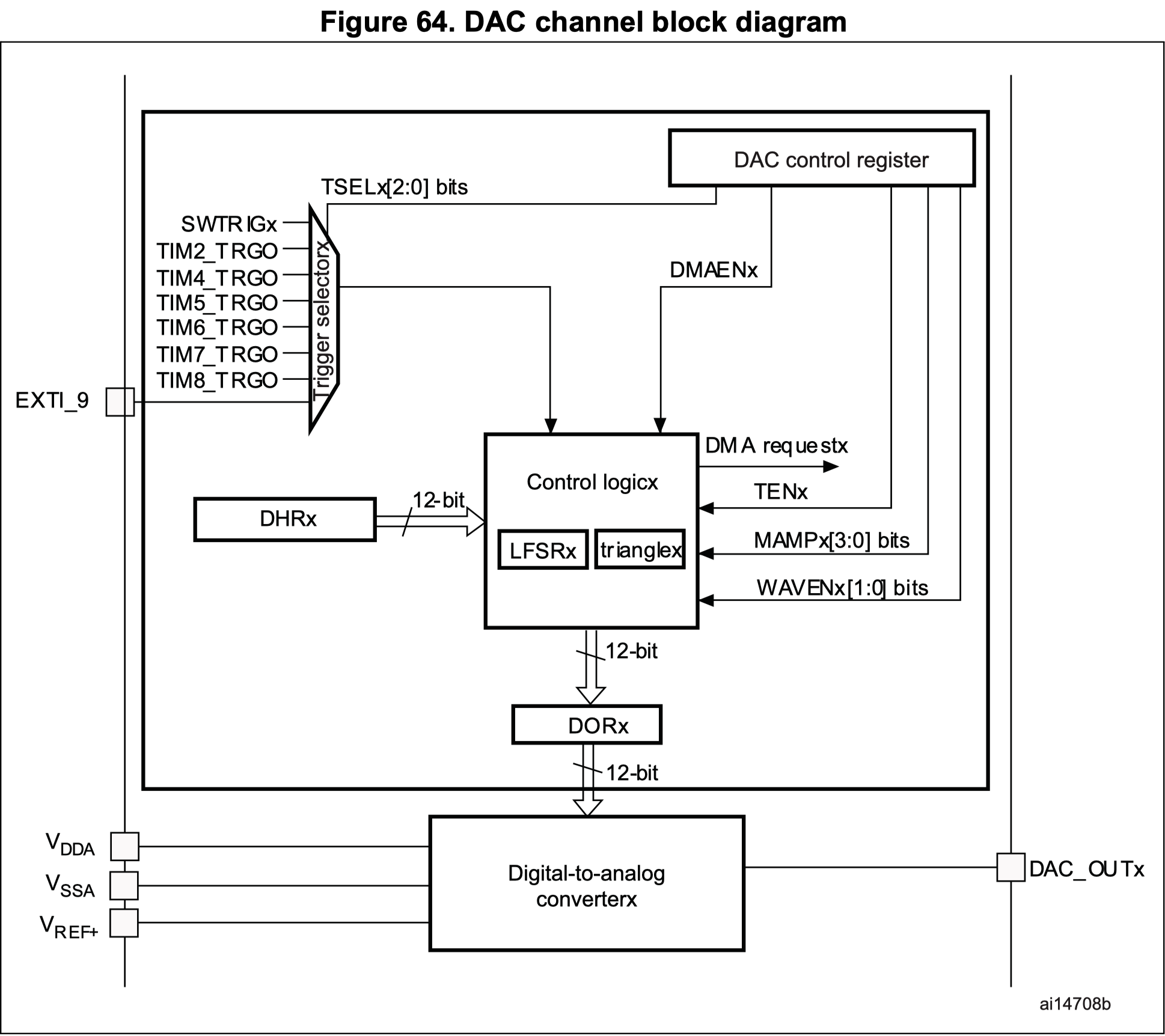
The DAC of the STM32 has three major trigger sources:
- Timer triggered.
- External Triggered.
- Software triggered.
In the previous guide, we covered the software trigger part.
For timer trigger, there are several options:
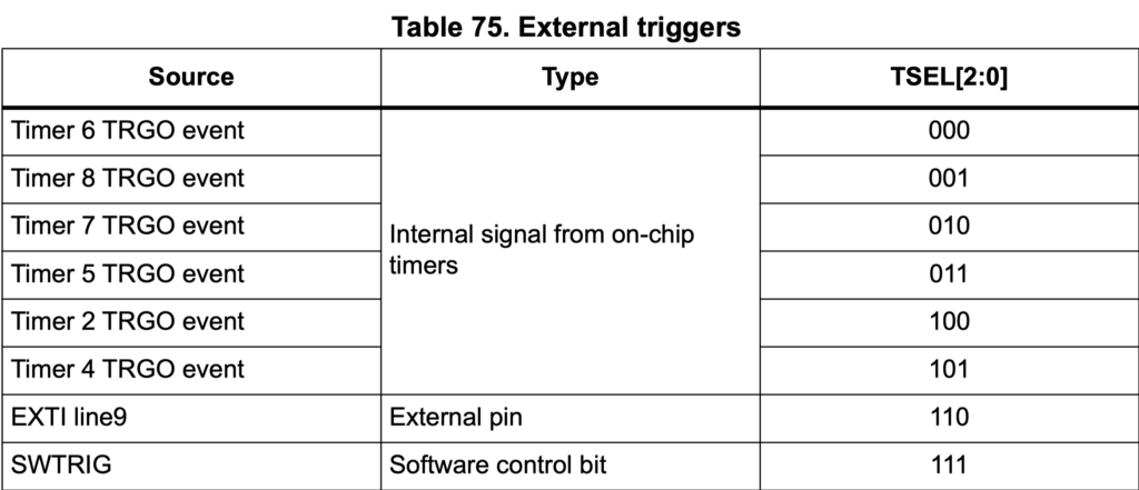
In this guide, we shall use timer6 to trigger the DAC.
2. DAC with timer trigger calculation:
Let’s say we’ve generated a sinewave lookup table with 128 sample points (Ns), and configured Timer2 so it triggers the DMA transfer to the DAC output. What would be the output sine wave frequency?
Here are the formulas to be used
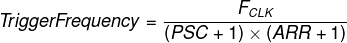
Where FCLK is the frequency of the clock used by your timer module, PSC is the Prescaler, and ARR is the value of the auto-reload register.

Where Ns is the sample points number in the lookup table.
For example, let’s assume the following settings:
The FCLK is 80MHz, the PSC is 0, ARR is 1000, and the sine lookup table has 128 sample points. What would be the output sine wave frequency?
TriggerFrequency = 80MHz / 1001 = 79920.08
Output Sinewave Frequency = TriggerFrequency / 128 = 624.37 Hz
3. Configuring DMA for DAC:
Before we configure the DMA, we need to get which DMA is responsible for DAC.
From STM32F407 Reference manual DMA section:
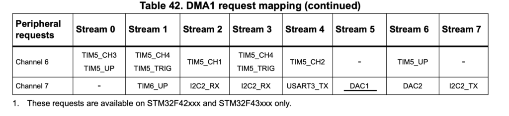
From the table, we can see that DMA1, Stream5 and channel 7 is responsible for DAC.
Hence we can start by creating macros for the channel number as following:
#define ch7 0x07
Then we enable clock access to DMA1 as following:
RCC->AHB1ENR|=RCC_AHB1ENR_DMA1EN;
Then we set the following:
- Channel to number 7.
- Memory and peripheral size to 16-bit (half-word).
- Memory increment.
- Circular mode
- Direction from memory to peripheral.
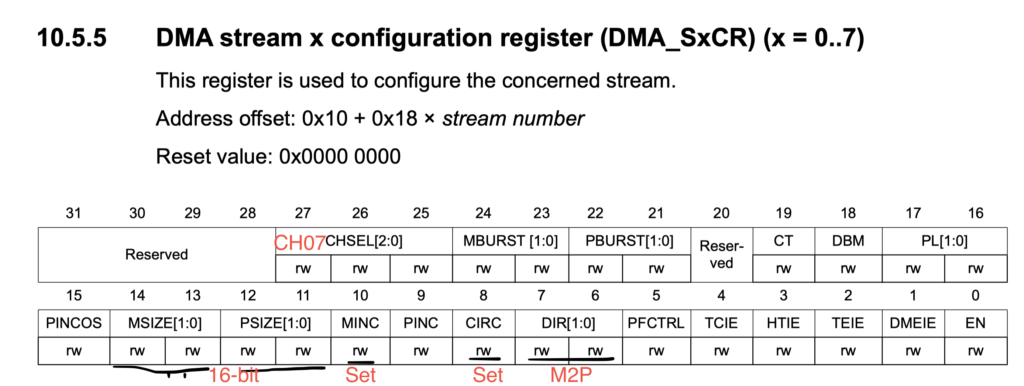
DMA1_Stream5->CR|=DMA_SxCR_MSIZE_0|DMA_SxCR_PSIZE_0|DMA_SxCR_MINC
|DMA_SxCR_CIRC|DMA_SxCR_DIR_0;
Then we set the number of transfer as following (128 in this case):
DMA1_Stream5->NDTR=128;
Then we set the peripheral and memory location as following:
DMA1_Stream5->PAR=(uint32_t)&(DAC->DHR12R1);
DMA1_Stream5->M0AR=(uint32_t)function;
Enable direct mode and FIFO threshold to full:
DMA1_Stream5->FCR |= DMA_SxFCR_DMDIS;
DMA1_Stream5->FCR |= (DMA_SxFCR_FTH_0 | DMA_SxFCR_FTH_1);
4. Configure TIM6 for DAC:
First we enable clock access to timer6 as following:
RCC->APB1ENR|=RCC_APB1ENR_TIM6EN;
We set the prescaler and ARR values as following:
TIM6->PSC=0;
TIM6->ARR=1;
Then set the update event is selected as a trigger output (TRGO) in CR2 as following:
TIM6->CR2|=TIM_CR2_MMS_1;
Then set the update event is selected as a trigger output (TRGO) in CR2 as following:
TIM6->CR2|=TIM_CR2_MMS_1;
5. Configuring DAC for DMA:
First thing enable clock access to DAC1 and GPIOA and set PA4 as analog mode:
RCC->AHB1ENR|=RCC_AHB1ENR_GPIOAEN;
RCC->APB1ENR|=RCC_APB1ENR_DACEN;
GPIOA->MODER|=GPIO_MODER_MODER4_0|GPIO_MODER_MODER4_1;
Configure the amplitude to be maximum of 4095:
DAC1->CR|=DAC_CR_MAMP1_3|DAC_CR_MAMP1_1|DAC_CR_MAMP1_0|DAC_CR_MAMP1_2;
Then select timer6 as trigger source as following:
DAC1->CR&=~(DAC_CR_TSEL1_0|DAC_CR_TSEL1_1|DAC_CR_TSEL1_2);
Enable DMA request as following:
DAC1->CR|=DAC_CR_DMAEN1;
Finally enable DAC then the DMA and finally the timer as following:
DAC1->CR|=DAC_CR_EN1;
DMA1_Stream5->CR|=DMA_SxCR_EN;
TIM6->CR1|=TIM_CR1_CEN;
Variables used for sinewave lookup table
#define   SINE_RES          128
const uint16_t function[SINE_RES] = { 2048, 2145, 2242, 2339, 2435, 2530, 2624, 2717, 2808, 2897,
                                      2984, 3069, 3151, 3230, 3307, 3381, 3451, 3518, 3581, 3640,
                                      3696, 3748, 3795, 3838, 3877, 3911, 3941, 3966, 3986, 4002,
                                      4013, 4019, 4020, 4016, 4008, 3995, 3977, 3954, 3926, 3894,
                                      3858, 3817, 3772, 3722, 3669, 3611, 3550, 3485, 3416, 3344,
                                      3269, 3191, 3110, 3027, 2941, 2853, 2763, 2671, 2578, 2483,
                                      2387, 2291, 2194, 2096, 1999, 1901, 1804, 1708, 1612, 1517,
                                      1424, 1332, 1242, 1154, 1068, 985, 904, 826, 751, 679,
                                      610, 545, 484, 426, 373, 323, 278, 237, 201, 169,
                                      141, 118, 100, 87, 79, 75, 76, 82, 93, 109,
                                      129, 154, 184, 218, 257, 300, 347, 399, 455, 514,
                                      577, 644, 714, 788, 865, 944, 1026, 1111, 1198, 1287,
                                      1378, 1471, 1565, 1660, 1756, 1853, 1950, 2047 };
6. Code:
The entire code as following:
#include "stm32f7xx.h"
#define ch7 0x07
#define   SINE_RES          128
const uint16_t function[SINE_RES] = { 2048, 2145, 2242, 2339, 2435, 2530, 2624, 2717, 2808, 2897,
                                      2984, 3069, 3151, 3230, 3307, 3381, 3451, 3518, 3581, 3640,
                                      3696, 3748, 3795, 3838, 3877, 3911, 3941, 3966, 3986, 4002,
                                      4013, 4019, 4020, 4016, 4008, 3995, 3977, 3954, 3926, 3894,
                                      3858, 3817, 3772, 3722, 3669, 3611, 3550, 3485, 3416, 3344,
                                      3269, 3191, 3110, 3027, 2941, 2853, 2763, 2671, 2578, 2483,
                                      2387, 2291, 2194, 2096, 1999, 1901, 1804, 1708, 1612, 1517,
                                      1424, 1332, 1242, 1154, 1068, 985, 904, 826, 751, 679,
                                      610, 545, 484, 426, 373, 323, 278, 237, 201, 169,
                                      141, 118, 100, 87, 79, 75, 76, 82, 93, 109,
                                      129, 154, 184, 218, 257, 300, 347, 399, 455, 514,
                                      577, 644, 714, 788, 865, 944, 1026, 1111, 1198, 1287,
                                      1378, 1471, 1565, 1660, 1756, 1853, 1950, 2047 };


int main(void)
{


	RCC->AHB1ENR|=RCC_AHB1ENR_GPIOAEN;
	RCC->APB1ENR|=RCC_APB1ENR_DACEN;
	RCC->APB1ENR|=RCC_APB1ENR_TIM6EN;
	RCC->AHB1ENR|=RCC_AHB1ENR_DMA1EN;

	DMA1_Stream5->CR&=~DMA_SxCR_EN;
	while(((DMA1_Stream5->CR)&DMA_SxCR_EN)==1);
	DMA1_Stream5->CR|=(ch7<<25);
	DMA1_Stream5->CR|=DMA_SxCR_MSIZE_0|DMA_SxCR_PSIZE_0|DMA_SxCR_MINC
	|DMA_SxCR_CIRC|DMA_SxCR_DIR_0;
	DMA1_Stream5->NDTR=128;
	DMA1_Stream5->PAR=(uint32_t)&(DAC->DHR12R1);
	DMA1_Stream5->M0AR=(uint32_t)function;

	DMA1_Stream5->FCR |= DMA_SxFCR_DMDIS;
	DMA1_Stream5->FCR |= (DMA_SxFCR_FTH_0 | DMA_SxFCR_FTH_1);

	TIM6->PSC=0;
	TIM6->ARR=1;
	TIM6->CR2|=TIM_CR2_MMS_1;

	GPIOA->MODER|=GPIO_MODER_MODER4;

	DAC1->CR|=DAC_CR_MAMP1_3|DAC_CR_MAMP1_1|DAC_CR_MAMP1_0|DAC_CR_MAMP1_2;
	DAC1->CR&=~(DAC_CR_TSEL1_0|DAC_CR_TSEL1_1|DAC_CR_TSEL1_2);
	DAC1->CR|=DAC_CR_DMAEN1;
	DAC1->CR|=DAC_CR_TEN1;
	//DAC1->CR|=DAC_CR_BOFF1;
	DAC1->CR|=DAC_CR_EN1;
	DMA1_Stream5->CR|=DMA_SxCR_EN;
	TIM6->CR1|=TIM_CR1_CEN;

while(1)
	{
		/*
		Do something else here
		*/
	}


}
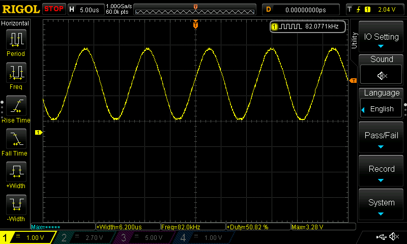
7. Results:
After compiling and uploading the code to STM32F7 and probe PA5 using oscilloscope, you should get this sinewave.
Happy coding 🙂
Add Comment