In this guide, we shall take a look at the internal DAC of STM32F767 and develop software triggered DAC to generate triangle wave.
In this guide, we shall cover the following:
- What is DAC
- Configure DAC
- Generate wave form from DAC
- Results
1 What is DAC:
In electronics, a digital-to-analog converter (DAC, D/A, D2A, or D-to-A) is a system that converts a digital signal into an analog signal. An analog-to-digital converter (ADC) performs the reverse function.
STM32 DAC Brief
In STM32F767, the DAC module is a 12-bit, voltage-output digital-to-analog converter. The DAC can be configured in 8- or 12-bit mode and may be used in conjunction with the DMA controller. In 12-bit mode, the data could be left- or right-aligned. The DAC features up to two output channels, each with its own converter. In dual DAC channel mode, conversions could be done independently or simultaneously when both channels are grouped together for synchronous update operations.
The DAC_OUTx pin can be used as general-purpose input/output (GPIO) when the DAC output is disconnected from the output pad and connected to on-chip peripherals. The DAC output buffer can be optionally enabled to allow a high drive output current. An individual calibration can be applied to each DAC output channel. The DAC output channels support a low power mode, the Sample and Hold mode.
DAC Features:
The two 12-bit buffered DAC channels can be used to convert two digital signals into two analog voltage signal outputs.
This dual digital Interface supports the following features:
• two DAC converters: one for each output channel
• 8-bit or 12-bit monotonic output
• left or right data alignment in 12-bit mode
• synchronized update capability
• noise-wave generation
• triangular-wave generation
• dual DAC channel independent or simultaneous conversions
• DMA capability for each channel
• external triggers for conversion
• input voltage reference V REF+
STM32 DAC Functional description:
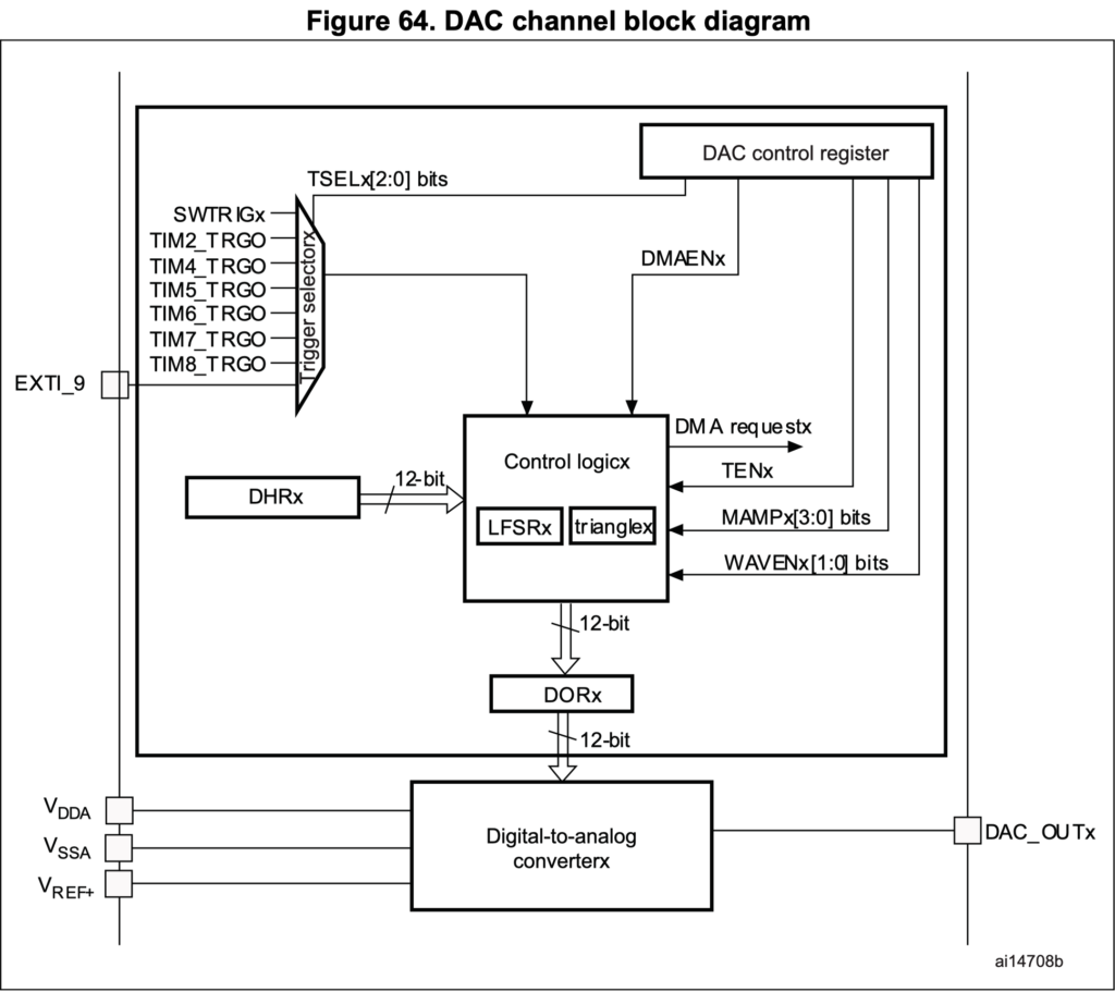
The DAC includes up to two separate output channels. Each output channel can be connected to on-chip peripherals such as comparator, operational amplifier, and ADC (if available). In this case, the DAC output channel can be disconnected from the DAC_OUTx output pin and the corresponding GPIO can be used for another purpose. The DAC output can be buffered or not.
Each DAC channel can be powered on by setting its corresponding ENx bit in the DAC_CR register. The DAC channel is then enabled after a tWAKEUP startup time.
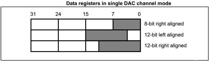
STM32 DAC Data Format
Depending on the selected configuration mode, the data have to be written into the specified register as described below:
Single DAC channel
There are three possibilities:
- 8-bit right alignment: the software has to load data into the DAC_DHR8Rx[7:0] bits (stored into the DHRx[11:4] bits)
- 12-bit left alignment: the software has to load data into the DAC_DHR12Lx [15:4] bits (stored into the DHRx[11:0] bits)
- 12-bit right alignment: the software has to load data into the DAC_DHR12Rx [11:0] bits (stored into the DHRx[11:0] bits)
Depending on the loaded DAC_DHRyyyx register, the data written by the user is shifted and stored into the corresponding DHRx (data holding registerx, which are internal non-memory mapped registers). The DHRx register is then loaded into the DORx register either automatically, by software trigger, or by an external event trigger.
STM32 DAC Conversion
The DAC_DORx cannot be written directly and any data transfer to the DAC channelx must be performed by loading the DAC_DHRx register (write operation to DAC_DHR8Rx, DAC_DHR12Lx, DAC_DHR12Rx, DAC_DHR8RD, DAC_DHR12RD or DAC_DHR12LD).
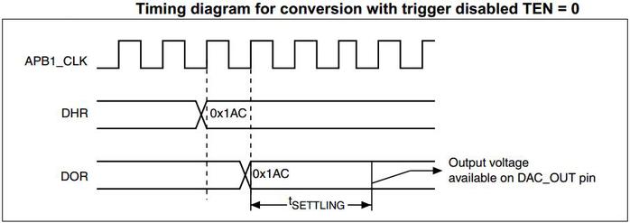
Data stored in the DAC_DHRx register are automatically transferred to the DAC_DORx register after one APB1 clock cycle if no hardware trigger is selected (TENx bit in DAC_CR register is reset). However, when a hardware trigger is selected (TENx bit in DAC_CR register is set) and a trigger occurs, the transfer is performed three APB1 clock cycles after the trigger signal.
When DAC_DORx is loaded with the DAC_DHRx contents, the analog output voltage becomes available after a time tSETTLING that depends on the power supply voltage and the analog output load.
STM32 DAC Output Voltage Equation (Formula)
Digital inputs are converted to output voltages on a linear conversion between 0 and VREF+. The analog output voltages on each DAC channel pin are determined by the following equation:
DACoutput = (VREF+) x (DOR/4096)
STM32 DAC Channel Modes of Operation
Each DAC channel can be configured in Normal mode or Sample and Hold mode. The output buffer can be enabled to allow a high drive capability. Before enabling the output buffer, the voltage offset needs to be calibrated. This calibration is performed at the factory (loaded after reset) and can be adjusted by software during application operation.
Normal Mode
In Normal mode, there are four combinations, by changing the buffer state, and by changing the DAC_OUTx pin interconnections.
To enable the output buffer, the MODEx[2:0] bits in DAC_MCR register should be:
- 000: DAC is connected to the external pin
- 001: DAC is connected to the external pin and to on-chip peripherals
To disable the output buffer, the MODEx[2:0] bits in DAC_MCR register should be:
- 010: DAC is connected to the external pin
- 011: DAC is connected to on-chip peripherals
Sample And Hold Mode
In sample and Hold mode, the DAC core converts data on a triggered conversion, then, holds the converted voltage on a capacitor. When not converting, the DAC cores and buffer are completely turned off between samples and the DAC output is tri-stated, therefore reducing the overall power consumption. A new stabilization period, which value depends on the buffer state, is required before each new conversion.
In this mode, the DAC core and all corresponding logic and registers are driven by the low-speed clock (LSI) in addition to the APB1 clock, allowing to use the DAC channels in deep low power modes such as Stop mode.
DAC Conversion On External Triggers
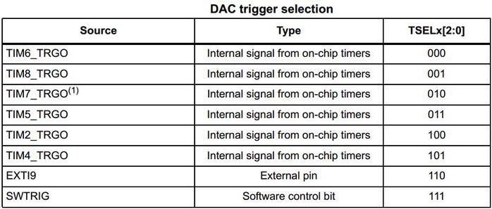
If the TENx control bit is set, conversion can then be triggered by an external event (timer counter, external interrupt line). The TSELx[2:0] control bits determine which out of 8 possible events will trigger conversion.
Each time a DAC interface detects a rising edge on the selected trigger source, the last data stored into the DAC_DHRx register are transferred into the DAC_DORx register. The DAC_DORx register is updated three APB1 cycles after the trigger occurs.
If the software trigger is selected, the conversion starts once the SWTRIG bit is set. SWTRIG is reset by hardware once the DAC_DORx register has been loaded with the DAC_DHRx register contents.
2. Configuring DAC of STM32F767:
Before we start configuring the DAC, we need to figure out which bus is the DAC is connected to and which pins.
From the datasheet of STM32F767:
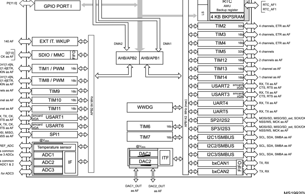
From the picture, we can see that DAC1 and DAC2 are connected to APB1, hence we can enable clock access to DAC as following:
RCC->APB1ENR|=RCC_APB1ENR_DACEN;
Now, we need to find which pins are connected to DAC1. This can be found also in the datasheet of F407:
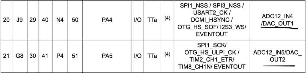
From the picture, we can conclude that PA4 and PA5 are the DAC output, since we need only single channel in this guide, we shall use PA4
Hence, we can enable clock access to GPIOA and set PA4 in analog mode as following:
RCC->AHB1ENR|=RCC_AHB1ENR_GPIOAEN;
GPIOA->MODER|=GPIO_MODER_MODER4_0|GPIO_MODER_MODER4_1;
ext, we start configure the DAC
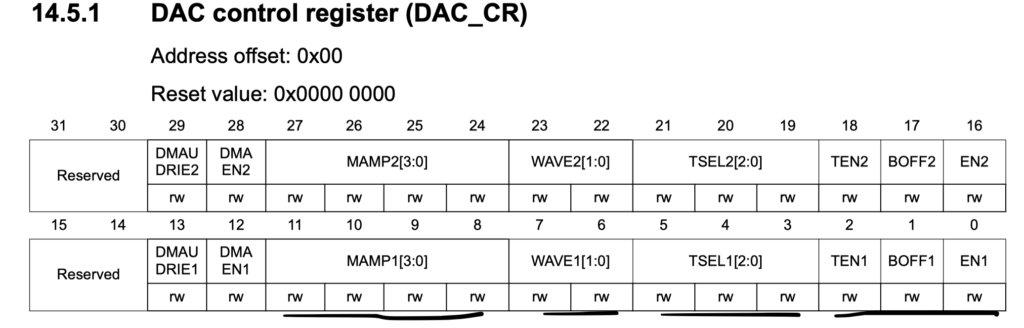
From the control register, we need to set as following:
- DAC channel1 mask/amplitude selector to 4096
- Wave1 to waveform mode
- Trigger source to software trigger
- Enable trigger
- Enable buffer and DAC channel1
DAC1->CR|=DAC_CR_MAMP1_3|DAC_CR_MAMP1_1|DAC_CR_MAMP1_0;
DAC1->CR|=DAC_CR_TSEL1_2|DAC_CR_TSEL1_1|DAC_CR_TSEL1_0;
DAC1->CR|=DAC_CR_TEN1;
DAC1->CR|=DAC_CR_BOFF1;
DAC1->CR|=DAC_CR_EN1;
3. Generate waveform from DAC:
We can generate waveform as following:
1. Write the value to DAC1->DHR12R1 register.
Trigger the DAC.
for (volatile int i=0;i<4095;i++)
				{
				DAC1->DHR12R1=i;
				DAC1->SWTRIGR|=DAC_SWTRIGR_SWTRIG1;

				}
Hence, the entire code as following:
#include "stm32f7xx.h"


int main(void)
{
RCC->AHB1ENR|=RCC_AHB1ENR_GPIOAEN;
RCC->APB1ENR|=RCC_APB1ENR_DACEN;
GPIOA->MODER|=GPIO_MODER_MODER4_0|GPIO_MODER_MODER4_1;
DAC1->CR|=DAC_CR_MAMP1_3|DAC_CR_MAMP1_1|DAC_CR_MAMP1_0;
DAC1->CR|=DAC_CR_TSEL1_2|DAC_CR_TSEL1_1|DAC_CR_TSEL1_0;
DAC1->CR|=DAC_CR_TEN1;
DAC1->CR|=DAC_CR_BOFF1;
DAC1->CR|=DAC_CR_EN1;


while(1)
	{

		for (volatile int i=0;i<4095;i++)
				{
				DAC1->DHR12R1=i;
				DAC1->SWTRIGR|=DAC_SWTRIGR_SWTRIG1;

				}


	}

}
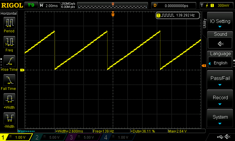
4. Result:
If you have an oscilloscope and probe pin PA4, you should see the following:
Happy coding 🙂
Add Comment