
In this revised version of SPI TX with DMA, we shall see how to transmit data over SPI using DMA.
In the previous guide (here), we discussed how to send a single character using SPI in polling mode. This method will decrease the CPU performance since the CPU has to wait for each time before sending the character. In this guide, we shall introduce DMA to send number of byte without blocking the operation of the CPU.
In this guide, we shall cover the following:
- SPI Pins initialization.
- SPI configuration.
- DMA configuration.
- SPI Interrupt handler
- SPI DMA send function.
- Header file.
- Main code.
- Results.
1. SPI initialization:
Create new source and header file with name of SPI.c and SPI.h respectively.
Within the source file:
Include the following header file:
#include "spi.h"

#include "stm32f4xx.h"
next, define a macros that will hold the alternate function number as mentioned here.
#define AF_SPI1 0x05
Declare the SPI pins initialization function:
void SPI1_Pins_Init(void)
Within the function:
- Enable clock access to GPIOA.
- Set PA5, PA6 and PA7 to alternate function.
- Select which alternate function to use.
void SPI1_Pins_Init(void)
{
	RCC->AHB1ENR|=RCC_AHB1ENR_GPIOAEN; //enable clock for GPIOA
	GPIOA->MODER|=GPIO_MODER_MODE5_1|GPIO_MODER_MODE6_1|GPIO_MODER_MODE7_1; //set PA5, PA6 and PA7 to alternate function mode
	GPIOA->MODER &=~(GPIO_MODER_MODE5_0|GPIO_MODER_MODE6_0|GPIO_MODER_MODE7_0);

	GPIOA->AFR[0]|=(AF_SPI1<<GPIO_AFRL_AFSEL5_Pos)|(AF_SPI1<<GPIO_AFRL_AFSEL6_Pos)|(AF_SPI1<<GPIO_AFRL_AFSEL7_Pos);
}
Now declare the following function which will initialize the SPI:
void SPI1_Init(void)
The SPI configuration as following:
In Control Register 1 (CR1):
- Enable Clock access to SPI
- Baud to be Fclk/8 (according to your application).
- CPOL and CPHA to 0 (according to your application also).
- Full duplex mode.
- Master Mode.
- Software slave management.
- 8-bit data mode.

	/*Enable clock access to SPI1 module*/
	RCC->APB2ENR |= RCC_APB2ENR_SPI1EN;

	/*Set clock to fPCLK/8*/
	SPI1->CR1 |=(SPI_CR1_BR_1);

	/*Set CPOL to 0 and CPHA to 0*/
	SPI1->CR1 &=~SPI_CR1_CPOL;
	SPI1->CR1 &=~SPI_CR1_CPHA;

	/*Enable full duplex*/
	SPI1->CR1 &=~SPI_CR1_RXONLY;

	/*Set MSB first*/
	SPI1->CR1 &= ~SPI_CR1_LSBFIRST;

	/*Set mode to MASTER*/
	SPI1->CR1 |= SPI_CR1_MSTR;

	/*Set 8 bit data mode*/
	SPI1->CR1 &= ~SPI_CR1_DFF;

	/*Select software slave management by
	* setting SSM=1 and SSI=1*/
	SPI1->CR1 |= SPI_CR1_SSI;
	SPI1->CR1 |= SPI_CR1_SSM;
In Control Register 2 (CR2):
Enable Tx buffer DMA enable:

	/*Enable SPI TX with DMA*/
	SPI1->CR2|=SPI_CR2_TXDMAEN;
Enable SPI interrupt in NVIC:
	/*Enable SPI1 Interrupt in NVIC*/
	NVIC_EnableIRQ(SPI1_IRQn);
Finally Enable SPI peripheral:
	/*Enable SPI module*/
	SPI1->CR1 |= SPI_CR1_SPE;
2. DMA Configuration:
Before the Initializing, we need to know which Stream and Channel is Connected to SPI_TX
According the figure below, we have two options, either Stream 5 or Stream 3 and both on Channel 3.
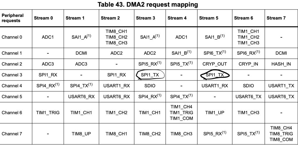
In our case, we shall use Stream 3.
Declare the following function will enable clock access to DMA2:
void DMA2_CLK_Init(void)
{
	/*Enable Clock access to DMA2*/
	RCC->AHB1ENR|=RCC_AHB1ENR_DMA2EN;
}
For the DMA2_Stream3 configuration:
- Channel number is 3.
- Direction is Memory to peripheral.
- Memory increment mode.
- Enable Transfer Complete Interrupt.
- Enable DMA2_Stream3 Interrupt in NVIC.
void DMA2_Stream3_CH2_Config(void)
{
	/*Disable the Stream and make sure it is disabled*/
	DMA2_Stream3->CR&=~DMA_SxCR_EN;

	while((DMA2_Stream3->CR)&DMA_SxCR_EN){;}

	/*Configure the DMA with the following parameters
	 *
	 * CH -> channel 3.
	 * Memory increment mode.
	 * Enable Transfer Complete interrupt
	 * */
  #define ch3		(0x03<<25)
	DMA2_Stream3->CR=ch3|DMA_SxCR_MINC|DMA_SxCR_DIR_0|DMA_SxCR_TCIE;

	/*Enable DMA2_Stream3 interrupt in NVIC*/
	NVIC_EnableIRQ(DMA2_Stream3_IRQn);

}
For DMA2_Stream3 Interrupt handler:
- Check if the source transfer complete, if it is, enable Tx Buffer empty interrupt for SPI1.
- Clear the pending flag.

void DMA2_Stream3_IRQHandler(void)
{
	if(DMA2->LISR&(DMA_LISR_TCIF3))
	{
		/*Enable SPI Tx buffer empty interrupt */

		SPI1->CR2|=SPI_CR2_TXEIE;

		/*Clear pending flag*/
		DMA2->LIFCR |=DMA_LIFCR_CTCIF3;
	}
}
3. SPI Interrupt Handler:
For the SPI interrupt handler:
Check if the source of the interrupt is Tx buffer is empty and the bus is not busy, it those two condition met:
- Call SPI_TX_Finished.
- Disable Tx buffer is empty interrupt.
__WEAK void SPI_TX_Finished(void)
{
	/*Override with user code*/
}

void SPI1_IRQHandler(void)
{
	if ((SPI1->SR & SPI_SR_TXE) && ((SPI1->SR & SPI_SR_BSY)==0))
	{
		/*Set finished to 1*/
		SPI_TX_Finished();

		/*Disable SPI Tx Buffer empty interrupt*/
		SPI1->CR2&=~SPI_CR2_TXEIE;


	}
}
Note: SPI_TX_Finished is defined as weak function and can be overridden by the user.
4. SPI DMA Send function:
Declare the following function:
void SPI1_TX_DMA(uint8_t *data,uint16_t len)
This function will send data using DMA over SPI and it takes two parameters:
- Pointer to the data to be sent.
- Length of the data.
Within the function:
- Clear transfer completed interrupt flag.
- Set the peripheral address to be SPI1->DR.
- Set the memory address to be the address of the data buffer.
- Number of transfer to be the length of the data.
- Enable the stream.
void SPI1_TX_DMA(uint8_t *data,uint16_t len)
{
	DMA2->LIFCR |=DMA_LIFCR_CTCIF3;
	DMA2_Stream3->PAR= (uint32_t)&SPI1->DR;
	DMA2_Stream3->M0AR=(uint32_t)data;
	DMA2_Stream3->NDTR=len;
	DMA2_Stream3->CR|=DMA_SxCR_EN;
}
Hence, the entire source code as following:
#include "spi.h"

#include "stm32f4xx.h"

#define AF_SPI1 0x05
#define ch3		(0x03<<25)


void SPI1_Pins_Init(void)
{
	RCC->AHB1ENR|=RCC_AHB1ENR_GPIOAEN; //enable clock for GPIOA
	GPIOA->MODER|=GPIO_MODER_MODE5_1|GPIO_MODER_MODE6_1|GPIO_MODER_MODE7_1; //set PA5, PA6 and PA7 to alternate function mode
	GPIOA->MODER &=~(GPIO_MODER_MODE5_0|GPIO_MODER_MODE6_0|GPIO_MODER_MODE7_0);

	GPIOA->AFR[0]|=(AF_SPI1<<GPIO_AFRL_AFSEL5_Pos)|(AF_SPI1<<GPIO_AFRL_AFSEL6_Pos)|(AF_SPI1<<GPIO_AFRL_AFSEL7_Pos);
}

void SPI1_Init(void)
{
	/*Enable clock access to SPI1 module*/
	RCC->APB2ENR |= RCC_APB2ENR_SPI1EN;

	/*Set clock to fPCLK/8*/
	SPI1->CR1 |=(SPI_CR1_BR_1);

	/*Set CPOL to 0 and CPHA to 0*/
	SPI1->CR1 &=~SPI_CR1_CPOL;
	SPI1->CR1 &=~SPI_CR1_CPHA;

	/*Enable full duplex*/
	SPI1->CR1 &=~SPI_CR1_RXONLY;

	/*Set MSB first*/
	SPI1->CR1 &= ~SPI_CR1_LSBFIRST;

	/*Set mode to MASTER*/
	SPI1->CR1 |= SPI_CR1_MSTR;

	/*Set 8 bit data mode*/
	SPI1->CR1 &= ~SPI_CR1_DFF;

	/*Select software slave management by
	* setting SSM=1 and SSI=1*/
	SPI1->CR1 |= SPI_CR1_SSI;
	SPI1->CR1 |= SPI_CR1_SSM;

	/*Enable SPI TX with DMA*/
	SPI1->CR2|=SPI_CR2_TXDMAEN;

	/*Enable SPI1 Interrupt in NVIC*/
	NVIC_EnableIRQ(SPI1_IRQn);

	/*Enable SPI module*/
	SPI1->CR1 |= SPI_CR1_SPE;
}

void spi1_transmit(uint8_t *data,uint32_t size)
{
	uint32_t i=0;

	while(i<size)
	{
		/*Wait until TXE is set*/
		while(!(SPI1->SR & (SPI_SR_TXE))){}

		/*Write the data to the data register*/
		SPI1->DR = data[i];
		i++;
	}
	/*Wait until TXE is set*/
	while(!(SPI1->SR & (SPI_SR_TXE))){}

	/*Wait for BUSY flag to reset*/
	while((SPI1->SR & (SPI_SR_BSY))){}

	/*Clear OVR flag*/
	(void)SPI1->DR;
	(void)SPI1->SR;
}

void spi1_receive(uint8_t *data,uint32_t size)
{
	while(size)
	{
		/*Send dummy data*/
		SPI1->DR =0;

		/*Wait for RXNE flag to be set*/
		while(!(SPI1->SR & (SPI_SR_RXNE))){}

		/*Read data from data register*/
		*data++ = (SPI1->DR);
		size--;
	}
}


void DMA2_CLK_Init(void)
{
	/*Enable Clock access to DMA2*/
	RCC->AHB1ENR|=RCC_AHB1ENR_DMA2EN;
}

void DMA2_Stream3_CH2_Config(void)
{
	/*Disable the Stream and make sure it is disabled*/
	DMA2_Stream3->CR&=~DMA_SxCR_EN;

	while((DMA2_Stream3->CR)&DMA_SxCR_EN){;}

	/*Configure the DMA with the following parameters
	 *
	 * CH -> channel 3.
	 * Memory increment mode.
	 * Enable Transfer Complete interrupt
	 * */
	DMA2_Stream3->CR=ch3|DMA_SxCR_MINC|DMA_SxCR_DIR_0|DMA_SxCR_TCIE;

	/*Enable DMA2_Stream3 interrupt in NVIC*/
	NVIC_EnableIRQ(DMA2_Stream3_IRQn);

}


void SPI1_TX_DMA(uint8_t *data,uint16_t len)
{
	DMA2->LIFCR |=DMA_LIFCR_CTCIF3;
	DMA2_Stream3->PAR= (uint32_t)&SPI1->DR;
	DMA2_Stream3->M0AR=(uint32_t)data;
	DMA2_Stream3->NDTR=len;
	DMA2_Stream3->CR|=DMA_SxCR_EN;
}

void DMA2_Stream3_IRQHandler(void)
{
	if(DMA2->LISR&(DMA_LISR_TCIF3))
	{

		/*Enable SPI Tx buffer empty interrupt */
		SPI1->CR2|=SPI_CR2_TXEIE;

		/*Clear pending flag*/
		DMA2->LIFCR |=DMA_LIFCR_CTCIF3;
	}
}


__WEAK void SPI_TX_Finished(void)
{
	/*Override with user code*/
}

void SPI1_IRQHandler(void)
{
	if ((SPI1->SR & SPI_SR_TXE) && ((SPI1->SR & SPI_SR_BSY)==0))
	{
		/*Set finished to 1*/
		SPI_TX_Finished();

		/*Disable SPI Tx Buffer empty interrupt*/
		SPI1->CR2&=~SPI_CR2_TXEIE;


	}
}
5. Header File:
The header file as following:
#ifndef SPI_H_
#define SPI_H_

#include "stdint.h"


void SPI1_Pins_Init(void);

void SPI1_Init(void);

void DMA2_CLK_Init(void);

void DMA2_Stream3_CH2_Config(void);

void SPI1_TX_DMA(uint8_t *data,uint16_t len);


#endif /* SPI_H_ */
6. Main Code:
In main.c:
#include "spi.h"
#include "stm32f4xx.h"

#define size_of_data 10

uint8_t data[size_of_data];

uint8_t finished_transfer=0;

int main(void)
{
	SPI1_Pins_Init();
	SPI1_Init();
	DMA2_CLK_Init();
	DMA2_Stream3_CH2_Config();

	/*Configure PA0 to act as CS pin*/
	RCC->AHB1ENR|=RCC_AHB1ENR_GPIOAEN;

	GPIOA->MODER|=GPIO_MODER_MODE0_0;
	GPIOA->MODER&=~GPIO_MODER_MODE0_1;

	GPIOA->BSRR=GPIO_BSRR_BS0;

	/*Fill the array with data from 0 to 9 for testing*/
	for (int i=0;i<size_of_data;i++)
	{
		data[i]=i;
	}

	while(1)
	{
		/*Set PA0 to low */
		GPIOA->BSRR=GPIO_BSRR_BR0;

		/*Send the data*/
		SPI1_TX_DMA(&data,size_of_data);

		/*Wait until the data have been transfer*/
		while(finished_transfer==0);

		/*Set PA0 to high*/
		GPIOA->BSRR=GPIO_BSRR_BS0;

		/*Reset the variable*/
		finished_transfer=0;

	}

}

void SPI_TX_Finished(void)
{
	finished_transfer=1;
}
7. Results:
After flashing the code to your STM32F4xx, connect logic analyzer to pins PA5, PA7 and PA0 and decode the SPI data, you should get the following:

Happy coding 😉
Add Comment