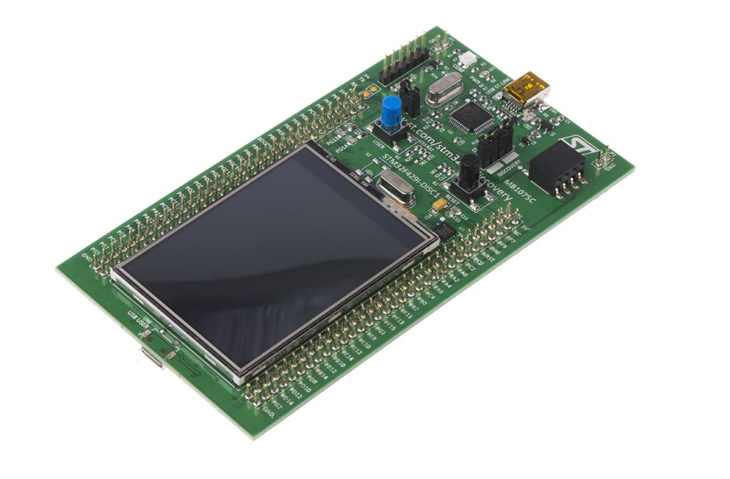
In this multipart guide, we shall focus on the display that embedded on STM32F429 discovery board and develop the driver for the LCD and the touch panel.
In part 1, we shall cover the following:
- Feature of the STM32F429 discovery.
- Environment setup.
1. Features of STM32F429 Discovery:
Features of STM32F429:
• STM32F429ZIT6 microcontroller featuring 2 Mbytes of Flash memory, 256 Kbytes of RAM in an LQFP144 package
• 2.4″ QVGA TFT LCD
• USB OTG with Micro-AB connector
• I3G4250D, ST MEMS motion sensor 3-axis digital output gyroscope
• Six LEDs:
– LD1 (red/green) for USB communication
– LD2 (red) for 3.3 V power-on
– Two user LEDs: LD3 (green), LD4 (red)
– Two USB OTG LEDs: LD5 (green) V BUS and LD6 (red) OC (over-current)
• Two push-buttons (user and reset)
• 64-Mbit SDRAM
• Extension header for LQFP144 I/Os for a quick connection to the prototyping board and an easy probing
• On-board ST-LINK/V2-B
• USB functions:
– Debug port
– Virtual COM port
– Mass storage
Since here we are focusing on the display part which is based on ILI9341, the display has the following features:
ILI9341 is a 262,144-color single-chip SOC driver for a-TFT liquid crystal display with resolution of 240RGBx320 dots, comprising a 720-channel source driver, a 320-channel gate driver, 172,800 bytes GRAM for graphic display data of 240RGBx320 dots, and power supply circuit.
ILI9341 supports parallel 8-/9-/16-/18-bit data bus MCU interface, 6-/16-/18-bit data bus RGB interface and 3-/4-line serial peripheral interface (SPI). The moving picture area can be specified in internal GRAM by window address function. The specified window area can be updated selectively, so that moving picture can be displayed simultaneously independent of still picture area.
ILI9341 can operate with 1.65V ~ 3.3V I/O interface voltage and an incorporated voltage follower circuit to generate voltage levels for driving an LCD. ILI9341 supports full color, 8-color display mode and sleep mode for precise power control by software and these features make the ILI9341 an ideal LCD driver for medium or small size portable products such as digital cellular phones, smart phone, MP3 and PMP where long battery life is a major concern.
Display resolution: [240xRGB](H) x 320(V) Output:
720sourceoutputs
320gateoutputs
Commonelectrodeoutput(VCOM)
a-TFT LCD driver with on-chip full display RAM: 172,800 bytes System Interface
- 8-bits, 9-bits, 16-bits, 18-bits interface with 8080- /8080- series MCU
- 6-bits,16-bits,18-bitsRGBinterfacewithgraphiccontroller
- 3-line/4-lineserialinterface Display mode:
Fullcolormode(IdlemodeOFF):262K-color(selectablecolordepthmodebysoftware) Reducecolormode(IdlemodeON):8-color Power saving mode: Sleepmode On chip functions:
VCOMgeneratorandadjustment
Timinggenerator
Oscillator
DC/DCconverter
Line/frameinversion
1presetGammacurvewithseparateRGBGammacorrection Content Adaptive Brightness Control MTP (3 times): 8-bitsforID1,ID2,ID3
7-bitsforVCOMadjustmen
Low -power consumption architecture Lowoperatingpowersupplies:
VDDI = 1.65V ~ 3.3V (logic)
VCI = 2.5V ~ 3.3V (analog) LCD Voltage drive:
Source/VCOMpowersupplyvoltage DDVDH – GND = 4.5V ~ 5.8V
VCL – GND = -1.5V ~ -2.5V
Gatedriveroutputvoltage
VGH – GND = 10.0V ~ 18.0V VGL – GND = -5.0V ~ -10.0V VGH – VGL 28V
VCOMdriveroutputvoltage
VCOMH = 3.0V ~ (DDVDH – 0.2)V VCOML = (VCL+0.2)V ~ 0V
VCOMH – VCOML 6.0V
Operate temperature range: -40 to 85
a-Si TFT LCD storage capacitor : Cst on Common structure only
2. Environment Setup:
We start by creating new STM32CubeIDE project for register level development.
Please refer to the following guide for the steps and modify the chip name from:
STM32F411xE
In symbolics to:
STM32F429xx
Now, create new source file with name of sys_init.c to configure the core to run at maximum 180MHz.
Follow this guide to see how to configure the core to run at maximum frequency using only register.
Within sys_init:
#include "stm32f4xx.h"

void SystemInit (void)
{

	#define PLL_M      4
	#define PLL_N      180
	#define PLL_P      2
	#define PLL_Q      9

	__IO uint32_t StartUpCounter = 0, HSEStatus = 0;


	  RCC->CR |= ((uint32_t)RCC_CR_HSEON);


	  do
	  {
		HSEStatus = RCC->CR & RCC_CR_HSERDY;
		StartUpCounter++;
	  } while((HSEStatus == 0) && (StartUpCounter != 3000));

	  if ((RCC->CR & RCC_CR_HSERDY) != RESET)
	  {
		HSEStatus = (uint32_t)0x01;
	  }
	  else
	  {
		HSEStatus = (uint32_t)0x00;
	  }

	  if (HSEStatus == (uint32_t)0x01)
	  {

		RCC->APB1ENR |= RCC_APB1ENR_PWREN;
		PWR->CR &= (uint32_t)~(PWR_CR_VOS);


		RCC->CFGR |= RCC_CFGR_HPRE_DIV1;


		RCC->CFGR |= RCC_CFGR_PPRE2_DIV1;


		RCC->CFGR |= RCC_CFGR_PPRE1_DIV2;


		RCC->PLLCFGR = PLL_M | (PLL_N << 6) | (((PLL_P >> 1) -1) << 16) |
					   (RCC_PLLCFGR_PLLSRC_HSE) | (PLL_Q << 24);


		RCC->CR |= RCC_CR_PLLON;


		while((RCC->CR & RCC_CR_PLLRDY) == 0)
		{
		}

		/* Configure Flash prefetch, Instruction cache, Data cache and wait state */
		FLASH->ACR = FLASH_ACR_ICEN |FLASH_ACR_DCEN |FLASH_ACR_LATENCY_5WS;

		/* Select the main PLL as system clock source */
		RCC->CFGR &= (uint32_t)((uint32_t)~(RCC_CFGR_SW));
		RCC->CFGR |= RCC_CFGR_SW_PLL;

		/* Wait till the main PLL is used as system clock source */
		while ((RCC->CFGR & (uint32_t)RCC_CFGR_SWS ) != RCC_CFGR_SWS_PLL)
		{;}
	  }
	  else
	  { /* If HSE fails to start-up, the application will have wrong clock
			 configuration. User can add here some code to deal with this error */
	  }

	  /*Enable FPU*/
	  SCB->CPACR |= ((3UL << 10*2)|(3UL << 11*2));
}
Before we continue, we need to find which SPI bus the LCD is connected.
From the STM32F429-Disco, we can find as following:
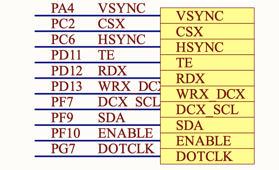
| STM32F429-disco | ILI9341 |
| PA7 | LCD RST |
| PC2 | LCD CS |
| PD13 | LCD DC |
| PF7 | SPI5 SCK |
| PF9 | SPI5 MOSI (SDA) |
Now, we create new header file with name of LCD_Pins.h .
Within the header file:
#ifndef LCD_PINS_H_
#define LCD_PINS_H_

#include "delay.h"


/*SPI */
void LCD_Pin_Init(void);
void LCD_SPI_Init(void);

/*LCD*/
void LCD_RST(void);
void LCD_Write_Cmd(uint8_t cmd);
void LCD_Write_Data (uint8_t data);


#endif /* LCD_PINS_H_ */
Now create source file with name of LCD_Pins.c:
Within the source file, include the following:
#include "stm32f4xx.h"
#include "LCD_Pins.h"
Declare the following symbolic for SPI5 as following:
#define AF05 0x05
Declare macros for setting the RST, CS and DC to either high or low.
We shall use atomic access to write to the pin using BSRR register:
#define LCD_RES_HIGH(void)			GPIOA->BSRR=GPIO_BSRR_BS7
#define LCD_RES_LOW(void)			GPIOA->BSRR=GPIO_BSRR_BR7

#define LCD_CS_HIGH(void)			GPIOC->BSRR=GPIO_BSRR_BS2
#define LCD_CS_LOW(void)			GPIOC->BSRR=GPIO_BSRR_BR2

#define LCD_DC_HIGH(void)			GPIOD->BSRR=GPIO_BSRR_BS13
#define LCD_DC_LOW(void)			GPIOD->BSRR=GPIO_BSRR_BR13
Initialize the pins:
void LCD_Pin_Init(void)
{
	RCC->AHB1ENR|=RCC_AHB1ENR_GPIOAEN|RCC_AHB1ENR_GPIOCEN|RCC_AHB1ENR_GPIODEN;

	/*PA7*/
	GPIOA->MODER|=GPIO_MODER_MODE7_0;
	GPIOA->MODER&=~GPIO_MODER_MODE7_1;
	GPIOA->OSPEEDR|=GPIO_OSPEEDR_OSPEED7;
	GPIOA->ODR|=GPIO_ODR_OD7;

	/*PC2*/
	GPIOC->MODER|=GPIO_MODER_MODE2_0;
	GPIOC->MODER&=~GPIO_MODER_MODE2_1;
	GPIOC->OSPEEDR|=GPIO_OSPEEDR_OSPEED2;
	GPIOC->ODR|=GPIO_ODR_OD2;


	/*PD13*/
	GPIOD->MODER|=GPIO_MODER_MODE13_0;
	GPIOD->MODER&=~GPIO_MODER_MODE13_1;
	GPIOD->OSPEEDR|=GPIO_OSPEEDR_OSPEED13;
	GPIOD->ODR|=GPIO_ODR_OD13;

	/*PF7 and PF9 for SPI5*/

	GPIOF->MODER|=GPIO_MODER_MODE7_1|GPIO_MODER_MODE9_1;
	GPIOF->MODER&=~(GPIO_MODER_MODE7_0|GPIO_MODER_MODE9_0);

	GPIOF->AFR[0]|=(AF05<<GPIO_AFRL_AFSEL7_Pos);
	GPIOF->AFR[1]|=(AF05<<GPIO_AFRH_AFSEL9_Pos);


}
Initialize SPI5 with following parameters:
- Master mode.
- Software slave management.
- Baudrate to be Fclk/8.
void LCD_SPI_Init(void)
{
	RCC->APB2ENR|=RCC_APB2ENR_SPI5EN;
	SPI5->CR1|=SPI_CR1_MSTR|SPI_CR1_SSM|SPI_CR1_SSI|
	SPI_CR1_BR_1;

	SPI5->CR1|=SPI_CR1_SPE;

}
Function that will write n byte using SPI bus and declared as static since no other function shall access this function:
static void spi5_transmit(uint8_t *data,uint32_t size)
{
	uint32_t i=0;


	while(i<size)
	{
		/*Wait until TXE is set*/
		while(!(SPI5->SR & (SPI_SR_TXE))){}

		/*Write the data to the data register*/
		SPI5->DR = data[i];
		i++;
	}
	/*Wait until TXE is set*/
	while(!(SPI5->SR & (SPI_SR_TXE))){}

	/*Wait for BUSY flag to reset*/
	while((SPI5->SR & (SPI_SR_BSY))){}

	/*Clear OVR flag*/
	(void) SPI5->DR;
	(void) SPI5->SR;
}
In order to reset the LCD, it needs the following steps:
- Set reset pin to low.
- Wait for 50 milliseconds.
- Set reset pin to high.
- Wait for 20 milliseconds.
void LCD_RST(void)
{
	LCD_RES_LOW();
	delay(50);
	LCD_RES_HIGH();
	delay(20);

}
Also, we need to write some commands to the LCD, we need the following steps:
- Set DC to low for command mode.
- Set CS to low to accept the SPI data.
- Write the command.
- Set CS back to high to indicate end of transmission.
void LCD_Write_Cmd(uint8_t cmd)
{
	LCD_CS_LOW();
	LCD_DC_LOW();
	spi5_transmit(&cmd,1);
	LCD_CS_HIGH();
}
To write the data, it is similar to writing command except that DC should be high:
void LCD_Write_Data (uint8_t data)
{
	LCD_CS_LOW();
	LCD_DC_HIGH();
	spi5_transmit (&data,1);
	LCD_CS_HIGH();
}
In part w2, we shall initialize the LCD and fill the screen with colors.
Stay tuned.
Add Comment