
In the previous guide of timer (here), we took a look at timer interrupt. In this guide, we shall see how to setup timer in PWM mode to fade an LED.
In this guide, we shall cover the following:
- What is PWM.
- Configure the timer and GPIO to generate PWM signal.
- Connection.
- Code.
- Demo.
1. What is PWM:
PWM is a technique used to emulate “analog signal” by rapidly turning on-off the pin. This allow the mcu to vary the power delivered to the load such as motor (will be covered later). The PWM has three main characteristics;
- Frequency:
which describe the duration time of the entire signal
- Duty cycle
The term duty cycle describes the proportion of ‘on’ time to the regular interval or ‘period’ of time; a low duty cycle corresponds to low power, because the power is off for most of the time. Duty cycle is expressed in percent, 100% being fully on.
- Amplitude
Which is the voltage level of the PWM (3.3v for STM32F1).
For more details, please check this wikipedia article (here).
2. Configure the timer and GPIO to generate PWM signal:
First, We need to decide on which timer to use since STM32F1 has multiple timers:
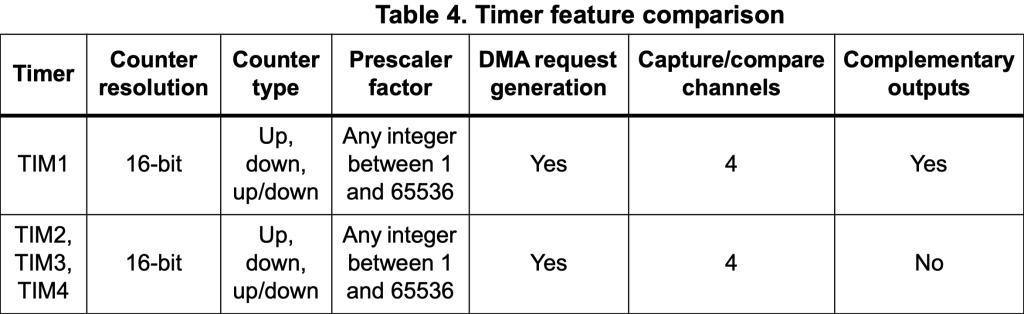
In this guide, we shall use TIM2.
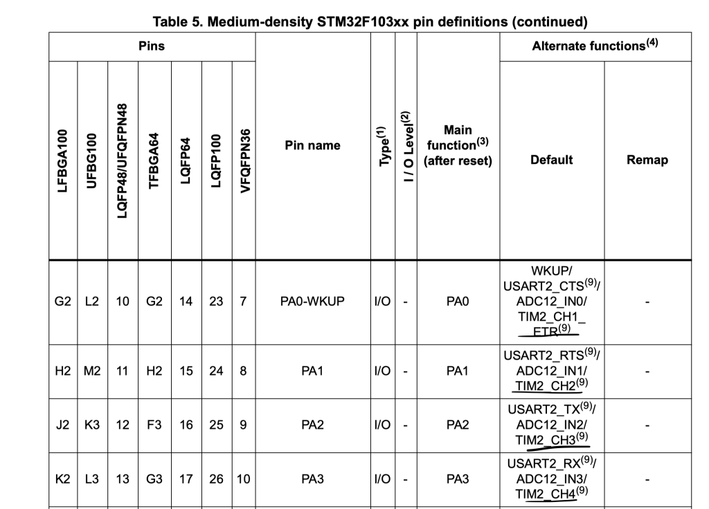
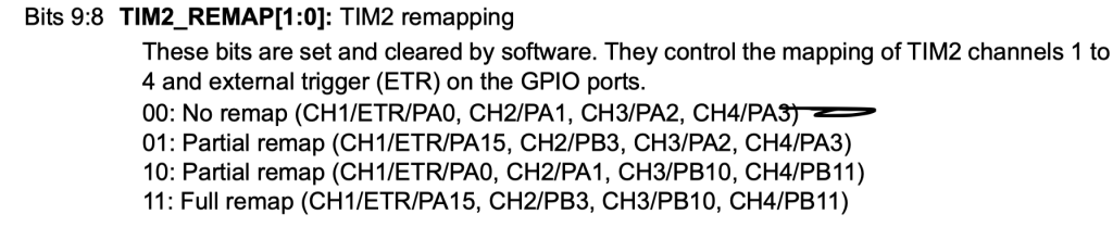
Now, we need to find which pins are connected to TIM2, from the datasheet, we can find that PA0 to PA3 are connected to TIM2_CH1 to TIM2CH4. In this guide, we are interested in TIM2_CH1, hence we need to configure PA0 as following:
- Output mode with maximum speed of 50MHz.
- Alternate Output Push/Pull mode.
First, we need to enable clock access to GPIOA:
RCC->APB2ENR|=RCC_APB2ENR_IOPAEN;
Then configure PA0:
	/*Configure PA0 as Output Alternate Push/Pull */
	GPIOA->CRL|=GPIO_CRL_MODE0;
	GPIOA->CRL|=(GPIO_CRL_CNF0_1);
	GPIOA->CRL&=~(GPIO_CRL_CNF0_0);
Finally, don’t remap to another pins:
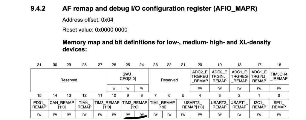
	/*Don't remap the pin*/
	AFIO->MAPR&=~AFIO_MAPR_TIM2_REMAP;
For the timer configuration, first enable clock access to TIM2 as following:
	/*Enable clock access to timer2*/
	RCC->APB1ENR|=RCC_APB1ENR_TIM2EN;
Set the prescaler and ARR to 0 and 100 respectively:
	/*Configure timer2*/
	TIM2->PSC=0;
	TIM2->ARR=100;
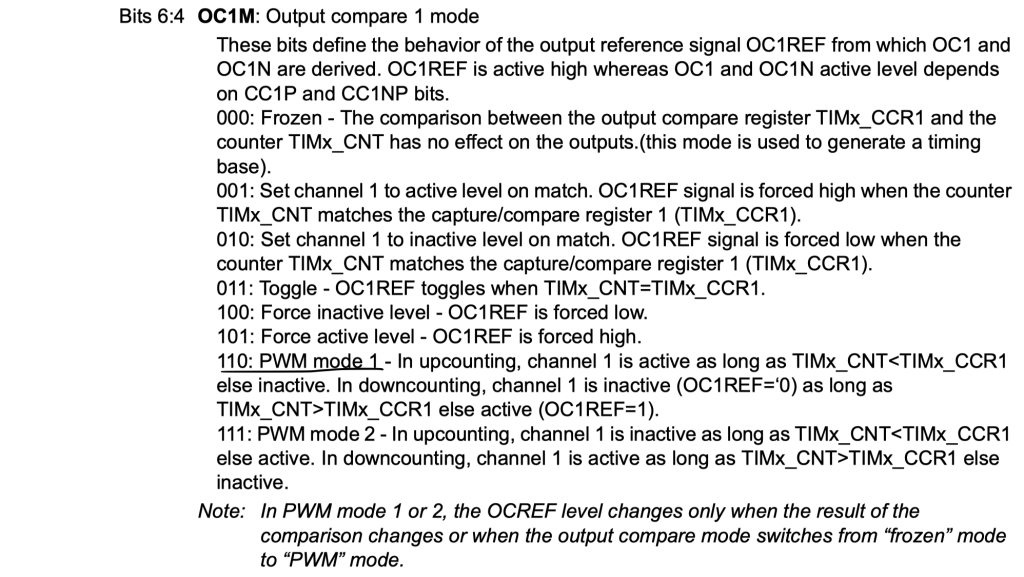
Now, in TIMx capture/compare mode register 1 which is responsible for CH1 and CH2, we need to set OC1M in PWM Mode as following:
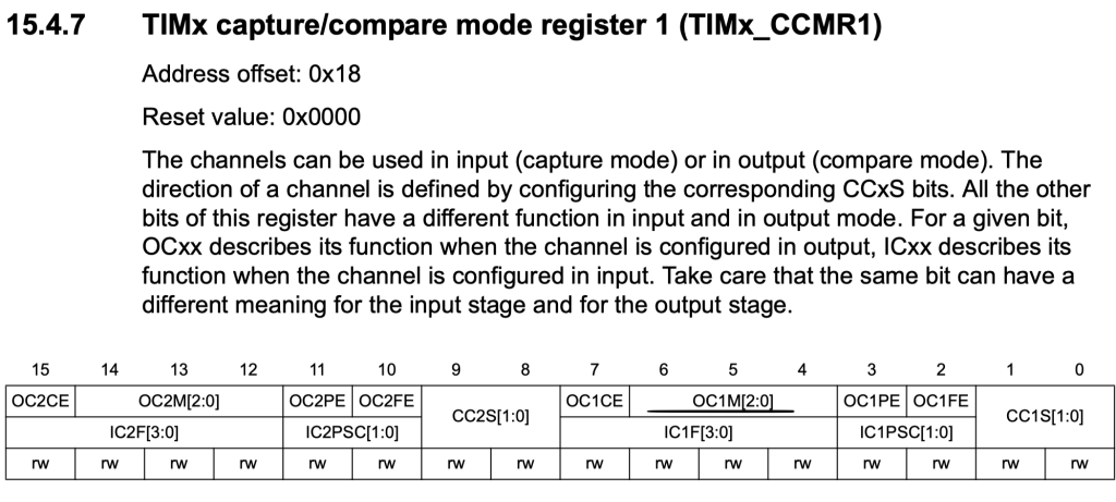
TIM2->CCMR1|=TIM_CCMR1_OC1M_2|TIM_CCMR1_OC1M_1;
Then enable the channel from TIMx capture/compare enable register (TIMx_CCER):
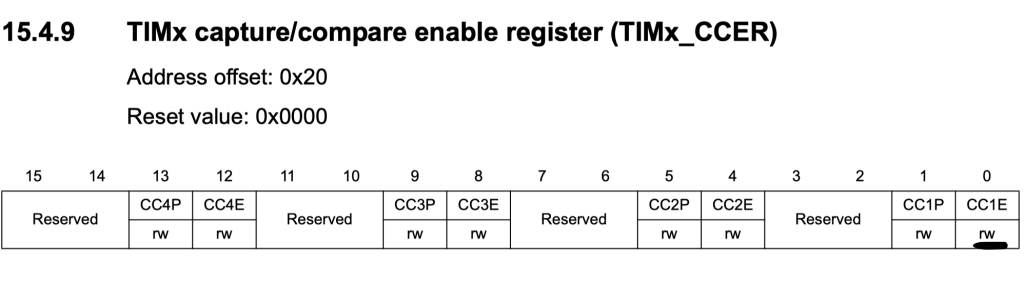
TIM2->CCER|=TIM_CCER_CC1E;
Finally, enable the timer:
TIM2->CR1|=TIM_CR1_CEN;
In order to vary the duty cycle, we need to write the value to the CCR1 register like this for example:
TIM2->CCR1=50; //50% duty cycle.
In this guide, the duty cycle is between 0 and 100 which means 0 is 0% and 100 is 100%.
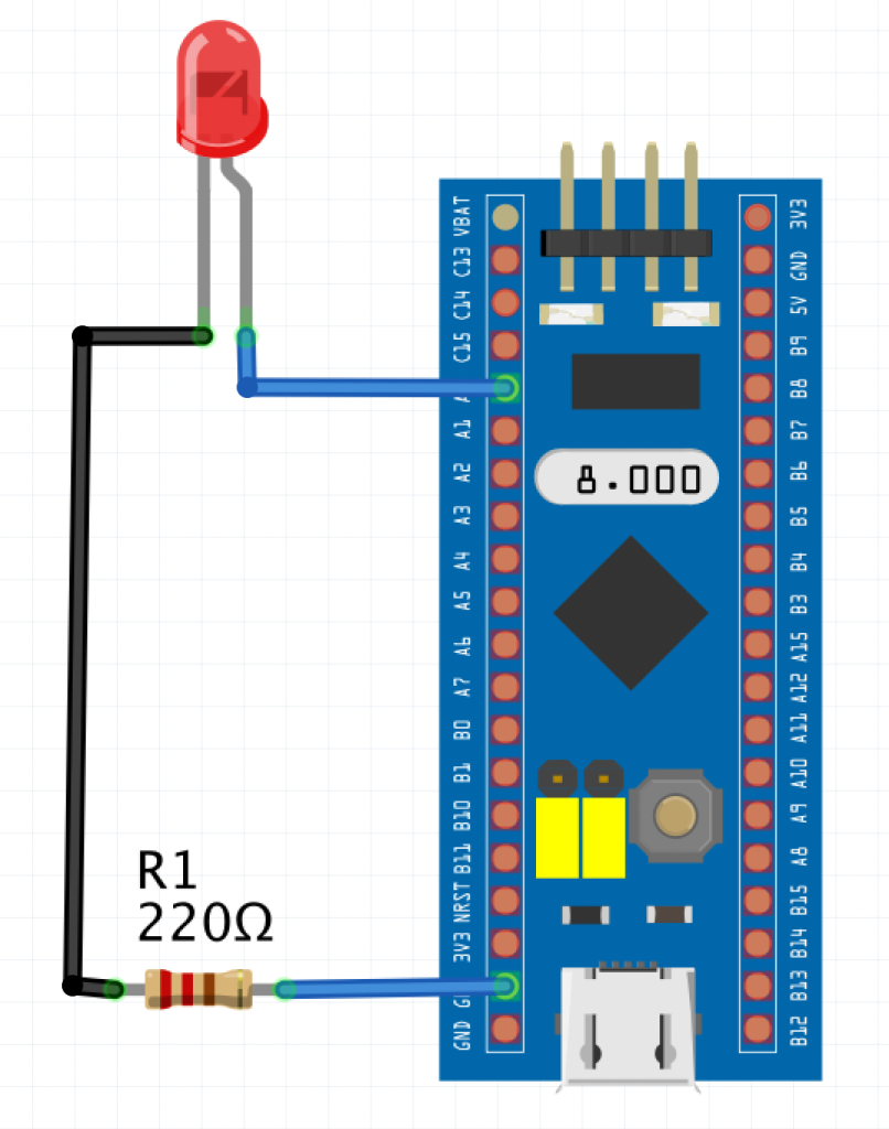
3. Connection:
The connection as following:
4. Code:
Hence, the entire code as following:
#include "stm32f1xx.h"

int main(void)
{
	RCC->APB2ENR|=RCC_APB2ENR_IOPAEN;

	/*Configure PA0 as Output Alternate Push/Pull */
	GPIOA->CRL|=GPIO_CRL_MODE0;
	GPIOA->CRL|=(GPIO_CRL_CNF0_1);
	GPIOA->CRL&=~(GPIO_CRL_CNF0_0);

	/*Don't remap the pin*/
	AFIO->MAPR&=~AFIO_MAPR_TIM2_REMAP;


	/*Enable clock access to timer2*/
	RCC->APB1ENR|=RCC_APB1ENR_TIM2EN;

	/*Configure timer2*/
	TIM2->PSC=0;
	TIM2->ARR=100;
	TIM2->CCMR1|=TIM_CCMR1_OC1M_2|TIM_CCMR1_OC1M_1;
	TIM2->CCER|=TIM_CCER_CC1E;
	TIM2->CR1|=TIM_CR1_CEN;

	while(1)
	{
		for (volatile int i=0;i<100;i++)
			{
				TIM2->CCR1=i;
				for (int j=0;j<10000;j++);
			}

		for (volatile int i=100;i>0;i--)
			{
				TIM2->CCR1=i;
				for (int j=0;j<10000;j++);
			}

	}
}
5. Demo:
Happy coding 🙂
2 Comments
Hi brother,
can you help me with same tutorial for the TIM1 how to use and set the dead time and how to make the pins as input and output at all.
i am using pin PA8,PA9 and PA10.
Thanks in advance
Hi,
wait for timer applications using HAL.
It will make your life easier.
Add Comment