In the previous guide (here), we took a look how to configure the ADC to work in continuous mode with single channel attached. In this guide we shall use DMA to acquire ADC data from two channels using DMA.
In this guide, we shall cover the following:
- What is DMA
- Why should we use DMA when dealing with multiple channel in ADC
- Required parts, schematics and connection
- Configuring the ADC and DMA
- Code
- Result
1. What is DMA
DMA which stands for Direct Memory Access is part of MCU that handle data transfer from peripheral to memory without invoking CPU at all which relief cpu to do something else, like processing the acquired adc vlaue for dsp processing etc
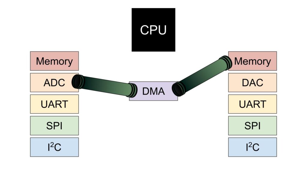
DMA can be operate in three different mode, Memory to Memory (moving one variable from one location to another), memory to peripheral (send string from memory to PC through UART) and peripheral to memory like in our case acquiring data from adc.
2. Why should we use DMA when dealing with multiple channel in ADC
Let say you want ti acquire data from adc from 3-channel in continuous mode. Since each conversion requires 15 cycles for 12-bit since the adc clock is the core frequency over (16MHz/2=8MHz), thats means generating interrupts at rate near half mega hertz which will effect the performance of the mcu. Hence, using DMA in such case makes sense.
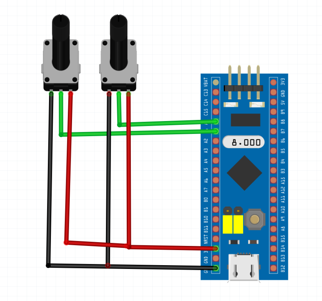
3. Required parts and connection:
The following are required:
- STM32F103C8.
- 2x 10KOhm potentiometer.
The connection as following:
4. Configuring ADC and DMA:
We start off by setting PA0 and PA1 as analog input:
- Enable clock access:
	//enable clock access to GPIOA
	RCC->APB2ENR|=RCC_APB2ENR_IOPAEN;
- Set PA0 and PA1 to analog mode:
	/*Set PA0 to analog Mode*/
	GPIOA->CRL&=~GPIO_CRL_CNF0;
	GPIOA->CRL&=~GPIO_CRL_MODE0;


	/*Set PA1 to analog Mode*/
	GPIOA->CRL&=~GPIO_CRL_CNF1;
	GPIOA->CRL&=~GPIO_CRL_MODE1;
Thats all for the pins section.
Now, we shall configure the ADC:
We start off by enabling clock access to the ADC1:
	/*Enable clock access to ADC1*/
	RCC->APB2ENR|=RCC_APB2ENR_ADC1EN;
Set trigger mode to be software trigger:
/*Set the trigger to be software mode*/
	ADC1->CR2 |= (7UL << ADC_CR2_EXTSEL_Pos);
Enable continuous mode:
	/*Enable Continuous mode */

	ADC1->CR2|=ADC_CR2_CONT;
Since we need multiple channel, we shall set scan bit in CR1 (Control Register 1) to 1:
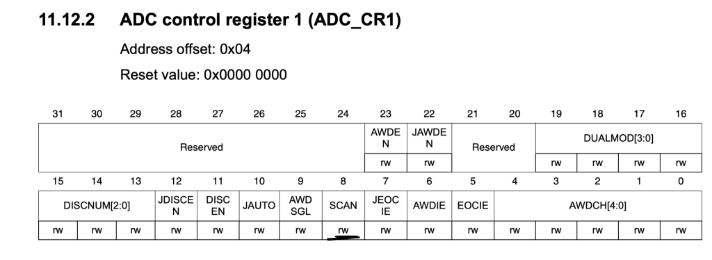
	/*Enable scan mode*/
	ADC1->CR1|=ADC_CR1_SCAN;
Also, enable DMA mode in CR2:
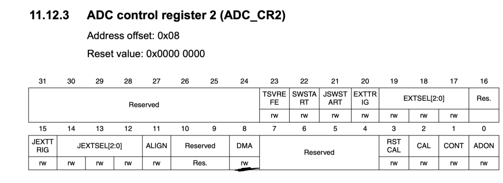
/*Enable DMA for ADC*/
ADC1->CR2|=ADC_CR2_DMA;
In scan mode, we need to tell the ADC the length of the sequence to be converted, which is in this case is 2:
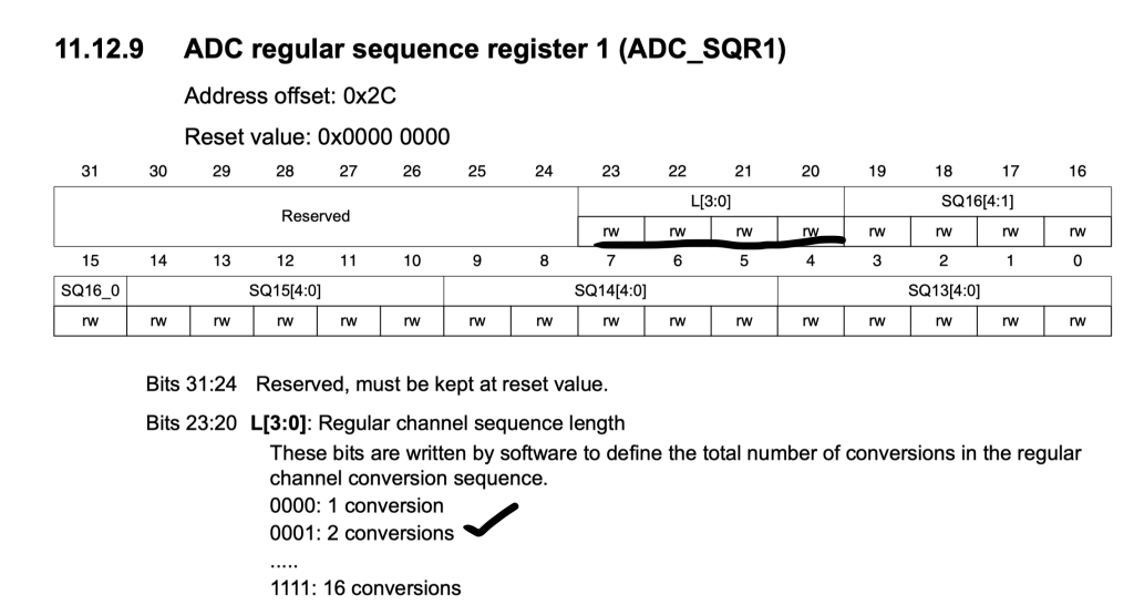
Hence, we can set the length to two as following:
#define ADC_Channels 	0x01
	/*Set length to 2*/
	ADC1->SQR1|=(ADC_Channels<<ADC_SQR1_L_Pos);
Then we shall set the sequence to be channel0 then channel1 as following:
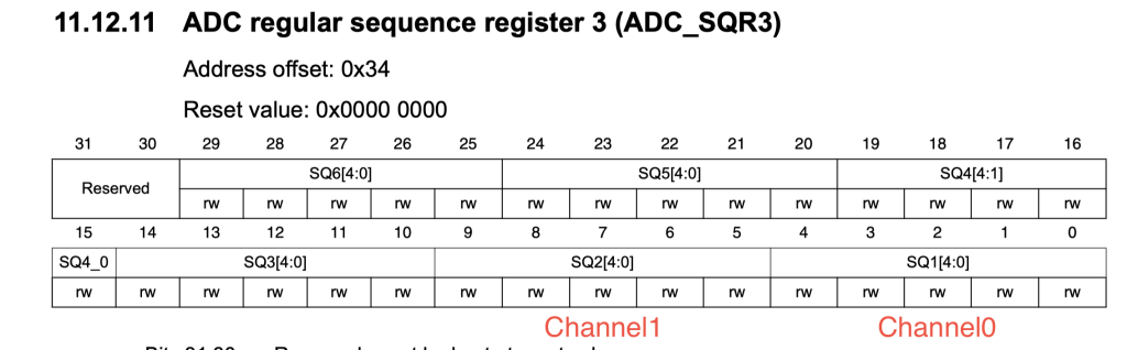
#define ADC_CH0			0x00 //PA0
#define ADC_CH1			0x01 //PA1

	/*Sample sequence
	 * PA0 then PA1
	 * */
	ADC1->SQR3|=(ADC_CH0<<ADC_SQR3_SQ1_Pos)|(ADC_CH1<<ADC_SQR3_SQ2_Pos);
Thats the configuration for ADC for now, noticed that we haven’t yet enable it since we need to configure the DMA before launching the ADC.
For the DMA Configuration, we need first to enable clock access to DMA as following:
	/*Enable Clock access to DMA1*/
	RCC->AHBENR|=RCC_AHBENR_DMA1EN;
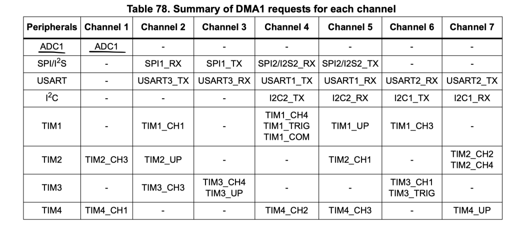
From DMA1 request map in reference manual, we find that DMA1_Channel1 is responsible for ADC1:
After that, the channel configuration as following:
- Memory and peripheral size to 16-bit (half word).
- Memory increment mode.
- Circular mode.
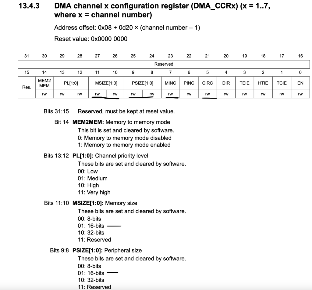
	DMA1_Channel1->CCR|=DMA_CCR_MSIZE_0|DMA_CCR_PSIZE_0|DMA_CCR_MINC
			|DMA_CCR_CIRC;
Set number if transfers to be 2:
DMA1_Channel1->CNDTR=2;
Set the peripheral address to be ADC1->DR:
DMA1_Channel1->CPAR=(uint32_t)(&ADC1->DR);
Set the memory address to be the array of two that will hold the ADC values:
DMA1_Channel1->CMAR=(uint32_t)(adc_data);
One last step before final step is to enable the DMA channel:
DMA1_Channel1->CCR|=DMA_CCR_EN;
Finally, enable the ADC and start conversion:
/*Power up the adc*/
	ADC1->CR2|=ADC_CR2_ADON;

	/*Wait a little bit*/

	for (int i=0;i<1000;i++);
	/*Launch the ADC*/
	ADC1->CR2|=ADC_CR2_ADON;

	/*Launch the ADC conversion*/
	ADC1->CR2|=ADC_CR2_SWSTART;
And while loop is empty
5. Code:
Hence, the code as following:
#include "stm32f1xx.h"


uint16_t adc_data[2];

#define ADC_Channels 	0x01

#define ADC_CH0			0x00 //PA0
#define ADC_CH1			0x01 //PA1


int main()
{
	/*Enable clock access to GPIOA*/
	//enable clock access to GPIOA
	RCC->APB2ENR|=RCC_APB2ENR_IOPAEN;
	/*Set PA0 to analog Mode*/
	GPIOA->CRL&=~GPIO_CRL_CNF0;
	GPIOA->CRL&=~GPIO_CRL_MODE0;


	/*Set PA1 to analog Mode*/
	GPIOA->CRL&=~GPIO_CRL_CNF1;
	GPIOA->CRL&=~GPIO_CRL_MODE1;


	/*Enable clock access to ADC1*/
	RCC->APB2ENR|=RCC_APB2ENR_ADC1EN;

	/*Set the trigger to be software mode*/
	ADC1->CR2 |= (7UL << ADC_CR2_EXTSEL_Pos);

	/*Enable Continuous mode */

	ADC1->CR2|=ADC_CR2_CONT;

	/*Enable scan mode*/
	ADC1->CR1|=ADC_CR1_SCAN;

	/*Enable DMA for ADC*/
	ADC1->CR2|=ADC_CR2_DMA;

	/*Set length to 2*/
	ADC1->SQR1|=(ADC_Channels<<ADC_SQR1_L_Pos);

	/*Sample sequence
	 * PA0 then PA1
	 * */
	ADC1->SQR3|=(ADC_CH0<<ADC_SQR3_SQ1_Pos)|(ADC_CH1<<ADC_SQR3_SQ2_Pos);

	/*DMA Related stuff*/

	/*Enable Clock access to DMA1*/
	RCC->AHBENR|=RCC_AHBENR_DMA1EN;

	/*DMA1_Channel1 is for ADC1*/

	DMA1_Channel1->CCR|=DMA_CCR_MSIZE_0|DMA_CCR_PSIZE_0|DMA_CCR_MINC
			|DMA_CCR_CIRC;

	DMA1_Channel1->CNDTR=2;

	DMA1_Channel1->CPAR=(uint32_t)(&ADC1->DR);

	DMA1_Channel1->CMAR=(uint32_t)(adc_data);

	DMA1_Channel1->CCR|=DMA_CCR_EN;

	/*Power up the adc*/
	ADC1->CR2|=ADC_CR2_ADON;

	/*Wait a little bit*/

	for (int i=0;i<1000;i++);
	/*Launch the ADC*/
	ADC1->CR2|=ADC_CR2_ADON;

	/*Launch the ADC conversion*/
	ADC1->CR2|=ADC_CR2_SWSTART;


	/*Blink PC13 to demonstrates DMA capabilities*/

	RCC->APB2ENR|=RCC_APB2ENR_IOPCEN;

	GPIOC->CRH|=GPIO_CRH_MODE13;
	GPIOC->CRH&=~(GPIO_CRH_CNF13);


	while(1)
	{
		GPIOC->ODR^=GPIO_ODR_ODR13;
		for(int i=0;i<100000;i++);

	}

}
6. Results:
Happy coding 🙂
2 Comments
Is ti possible to enable the DMA Interrupt (transfer complete flag) on this code?
Hi,
yes you can.
Add Comment