
In the previous guide (here), we took a look at the SPI transmit mode using DMA. In this guide, we shall use DMA to send and receive data from slave device (MPU9250) in this case using only DMA.
In the guide we will cover the following:
- SPI configuration for DMA
- DMA cofinguration
- SPI-TX and SPI-RX code
- Connection
- Code
- Demo
1. SPI configuration for DMA:
From the previous guide (Working with STM32 and SPI : Send bytes using DMA) we can grab the initialization function for the SPI clock, pins as following:
		#define ch3		(0x03<<25)
		#define AF05  (0x05)
		//enable clock for GPIOA
		RCC->AHB1ENR|=RCC_AHB1ENR_GPIOAEN;
			//set PA5, PA6 and PA7 to alternate function mode
		GPIOA->MODER|=GPIO_MODER_MODE5_1|GPIO_MODER_MODE6_1|GPIO_MODER_MODE7_1;
			//set which type of alternate function is
		GPIOA->AFR[0]|=(AF05<<20)|(AF05<<24)|(AF05<<28);
			//enable clock access to SPI1
		RCC->APB2ENR|=RCC_APB2ENR_SPI1EN;
			//set software slave managment
		SPI1->CR1|=SPI_CR1_SSM|SPI_CR1_SSI;
			//set SPI in master mode
		SPI1->CR1|=SPI_CR1_MSTR;
		SPI1->CR1|=SPI_CR1_BR_0|SPI_CR1_CPHA|SPI_CR1_CPOL;
From control register 2 (CR2) we can enable DMA for TX and RX as following:
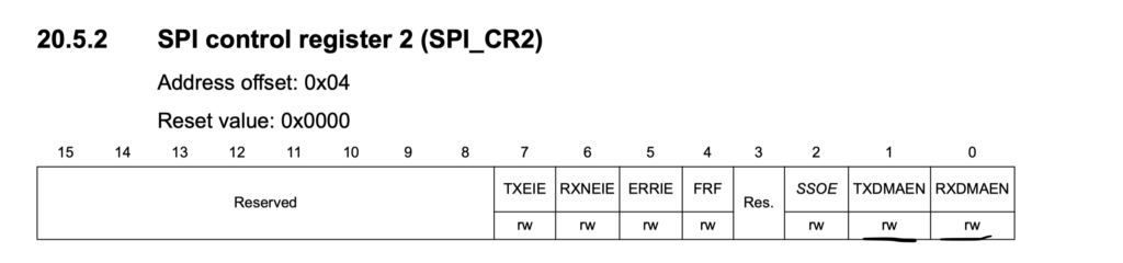
			//enable DMA_TX DMA_RX buffer
		SPI1->CR2|=SPI_CR2_TXDMAEN|SPI_CR2_RXDMAEN;
And finally enable SPI
			//enable SPI peripheral
		SPI1->CR1|=SPI_CR1_SPE;
2. DMA configuration:
Before we start configuring the DMA, we need to check which channel and stream for the SPI_TX and SPI_RX.
From the DMA section table 28 in reference manual of STM32F411, we can find which stream and channel.
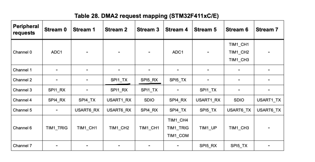
Sine we have multiple streams and channel, we shall use Stream2 and Stream3 and the channel shall be 3.
Hence we create symbolic name for channel3 as following:
#define ch3 (0x03<<25)
For SPI_TX we shall use DM2_Stream3
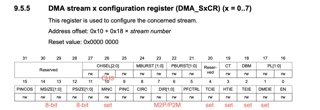
For DMA configuration, we need to configure the DMA with the following paramters:
- Channel: Channel 3.
- Memory and Peripheral size to 8-bit.
- Memory increment.
- Direction: Memory to peripheral.
- Enable transfer complete, half transfer transfer error and direct mode error interrupt and we don’t need to enable the Stream yet.
		//SPI_TX
void dma2_stream3_ch3_init(void)
	{
	RCC->AHB1ENR|=RCC_AHB1ENR_DMA2EN;
	DMA2_Stream3->CR&=~DMA_SxCR_EN;
	while((DMA2_Stream3->CR)&DMA_SxCR_EN){;}
	DMA2_Stream3->CR=ch3|DMA_SxCR_MINC|DMA_SxCR_DIR_0|DMA_SxCR_TCIE
	|DMA_SxCR_HTIE|DMA_SxCR_TEIE|DMA_SxCR_DMEIE;
	DMA2_Stream3->FCR |= DMA_SxFCR_DMDIS;
  DMA2_Stream3->FCR |= (DMA_SxFCR_FTH_0 | DMA_SxFCR_FTH_1);

	NVIC_EnableIRQ(DMA2_Stream3_IRQn);

	}
For SPI_RX we shall use Stream2 with the following configuration:
//SPI_RX
	void dma2_stream2_ch3_init(void)
	{
	RCC->AHB1ENR|=RCC_AHB1ENR_DMA2EN;
	DMA2_Stream2->CR&=~DMA_SxCR_EN;
	while((DMA2_Stream2->CR)&DMA_SxCR_EN){;}
	DMA2_Stream2->CR=ch3|DMA_SxCR_MINC|DMA_SxCR_TCIE
	|DMA_SxCR_HTIE|DMA_SxCR_TEIE|DMA_SxCR_DMEIE;
	DMA2_Stream2->FCR |= DMA_SxFCR_DMDIS;
  DMA2_Stream2->FCR |= (DMA_SxFCR_FTH_0 | DMA_SxFCR_FTH_1);
	NVIC_EnableIRQ(DMA2_Stream2_IRQn);

	}
3. SPI_TX and SPI_RX code:
For transferring data, first declare a function that takes two arguments:
- Source
- Length
void spi_transfer_dma(uint32_t src,uint32_t len){Inside the function, first clear all pending flags:
DMA2->LIFCR |=DMA_LIFCR_CTCIF3|DMA_LIFCR_CHTIF3|DMA_LIFCR_CTEIF3|DMA_LIFCR_CDMEIF3|DMA_LIFCR_CFEIF3;
Then set the peripheral address to be SPI->DR
DMA2_Stream3->PAR= (uint32_t)&(SPI1->DR);
Memory0 location to be the source (src):
DMA2_Stream3->M0AR=src;
Number of transfer to be length:
DMA2_Stream3->NDTR=len;
Finally enable the stream
DMA2_Stream3->CR|=DMA_SxCR_EN;
}
For SPI_RX, the code shall be:
void spi_receive_dma (uint32_t dest,uint32_t len)
				{
				DMA2->LIFCR |=DMA_LIFCR_CTCIF2|DMA_LIFCR_CHTIF2|DMA_LIFCR_CTEIF2|DMA_LIFCR_CDMEIF2|DMA_LIFCR_CFEIF2;

				DMA2_Stream2->PAR= (uint32_t)&(SPI1->DR);
				DMA2_Stream2->M0AR=dest;
				DMA2_Stream2->NDTR=len;
				DMA2_Stream2->CR|=DMA_SxCR_EN;
				}
Finally, Interrupt handling:
void DMA2_Stream3_IRQHandler(void)
		{

		if(DMA2->LISR&(DMA_LISR_TCIF3))
				{
					tx_finished=1;

					DMA2_Stream3->CR&=~DMA_SxCR_EN;

					DMA2->LIFCR |=DMA_LIFCR_CTCIF3;
				}

		if(DMA2->LISR&(DMA_LISR_HTIF3))
				{


					DMA2->LIFCR |=DMA_LIFCR_CHTIF3;
				}


		if(DMA2->LISR&(DMA_LISR_TEIF3))
						{

						DMA2->LIFCR|=(DMA_LIFCR_CTEIF3);
						}

		if(DMA2->LISR&(DMA_LISR_DMEIF3))
						{

						DMA2->LIFCR|=(DMA_LIFCR_CDMEIF3);
						}

		if(DMA2->LISR&(DMA_LISR_FEIF3))
						{

						DMA2->LIFCR|=(DMA_LIFCR_CFEIF0);
						}
			NVIC_ClearPendingIRQ(DMA2_Stream3_IRQn);

		}


void DMA2_Stream2_IRQHandler(void)
		{

		if(DMA2->LISR&(DMA_LISR_TCIF2))
				{
					rx_finished=1;

					DMA2_Stream2->CR&=~DMA_SxCR_EN;

					DMA2->LIFCR |=DMA_LIFCR_CTCIF2;
				}

		if(DMA2->LISR&(DMA_LISR_HTIF2))
				{


					DMA2->LIFCR |=DMA_LIFCR_CHTIF2;
				}


		if(DMA2->LISR&(DMA_LISR_TEIF2))
						{

						DMA2->LIFCR|=(DMA_LIFCR_CTEIF2);
						}

		if(DMA2->LISR&(DMA_LISR_DMEIF2))
						{

						DMA2->LIFCR|=(DMA_LIFCR_CDMEIF2);
						}

		if(DMA2->LISR&(DMA_LISR_FEIF2))
						{

						DMA2->LIFCR|=(DMA_LIFCR_CFEIF2);
						}

			NVIC_ClearPendingIRQ(DMA2_Stream2_IRQn);
		}
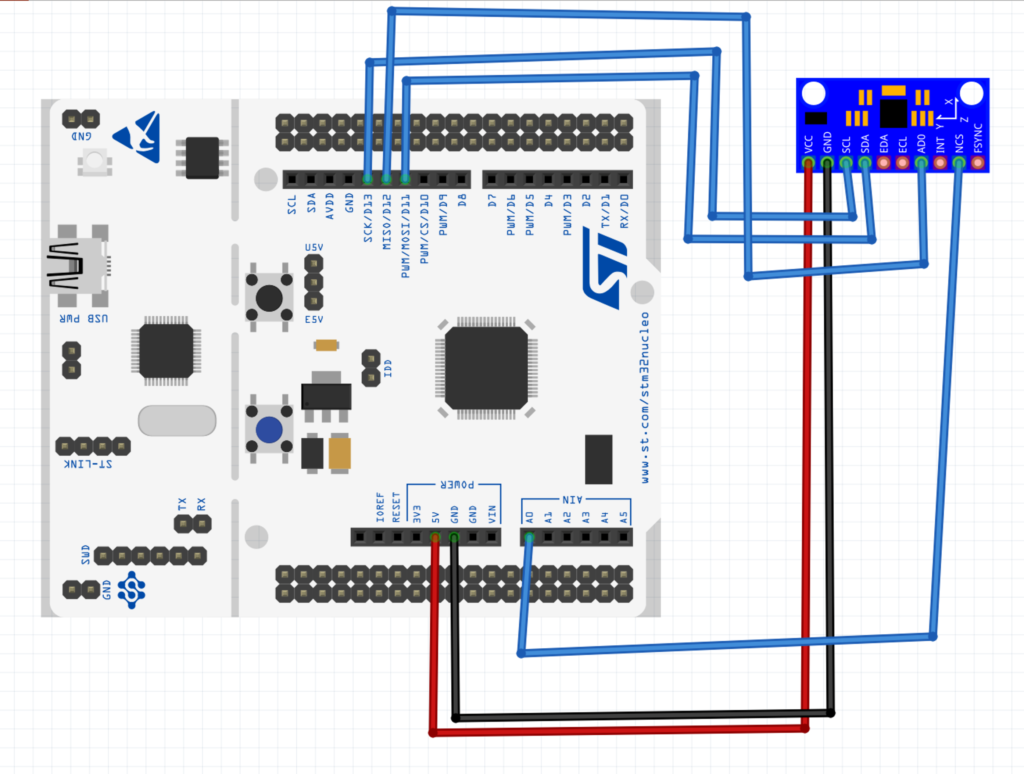
4. Connection:
Required parts:
- STM32F411RE Nucleo
- MPU9250 breakout
- hookup wires
For the connection of MPU9250 in the SPI mode, the module breakout shall be connect as following:
5. Code:
In order to read from MPU9250 we need to initialize it first as following:
uint8_t data[2];
double accelRange,gyroRange;
#define maximum_transfer 6
static uint8_t dummy_buffer[maximum_transfer];
char accelBuf[maximum_transfer+1];
volatile uint8_t tx_finished,rx_finished;
#define READ_FLAG   0x80

void MPU9250_beginAccel(uint8_t mode) {
  switch(mode) {
  case ACC_FULL_SCALE_2_G:
    accelRange = 2.0;
    break;
  case ACC_FULL_SCALE_4_G:
    accelRange = 4.0;
    break;
  case ACC_FULL_SCALE_8_G:
    accelRange = 8.0;
    break;
  case ACC_FULL_SCALE_16_G:
    accelRange = 16.0;
    break;
  default:
    return; // Return without writing invalid mode
  }

	data[0]=USER_CTRL; data[1]=(1<<4);
	spi_transfer_dma((uint32_t)data,2);
	while(tx_finished==0){;}
		tx_finished=0;

	data[0]=MPU9250_ADDR_ACCELCONFIG; data[1]=mode;
	spi_transfer_dma((uint32_t)data,2);
	while(tx_finished==0){;}
		tx_finished=0;
}
To update the values:
uint8_t MPU9250_accelUpdate(void) {
	dummy_buffer[0]=0x3B|READ_FLAG;

	spi_receive_dma(accelBuf,7);
	spi_transfer_dma(dummy_buffer,7);
	while(rx_finished==0){;}
	rx_finished=0;
	return 0;
}
Notice first we need to set the DMA to receive data first before we can transmit the read request
You may download the code from here:
6. Demo:
After you compile and upload the code. Add acc_x,acc_y,acc_z to watch window you should get similar results to the video when rotation the MPU9250 (This is for the acceleration part only).
Happy coding 🙂
4 Comments
Dear Sir,
Good Morning,
In this STM32F411RE’s SPI-DMA-Example,
While Comparing the same code with STM32L053, Same Routine
has the following lines (1-4) Missing,
what is the sanctity behind adding these Lines,
Please Let me know,
If I am wrongly comparing two different MCU’s.
thanks with regards,
HSR-Rao.
void MPU9250_beginAccel(uint8_t mode) {
switch(mode) {
case ACC_FULL_SCALE_2_G: accelRange = 2.0; break;
case ACC_FULL_SCALE_4_G: accelRange = 4.0; break;
case ACC_FULL_SCALE_8_G: accelRange = 8.0; break;
case ACC_FULL_SCALE_16_G: accelRange = 16.0; break;
default: return; // Return without writing invalid mode
}
01 | data[0]=USER_CTRL; data[1]=(1<<4);
02 | spi_transfer_dma((uint32_t)data,2);
03 | while(tx_finished==0){;}
04 | tx_finished=0;
data[0]=MPU9250_ADDR_ACCELCONFIG; data[1]=mode;
spi_transfer_dma((uint32_t)data,2);
while(tx_finished==0){;}
tx_finished=0;
}
Hi,
going through both codes, they are identical.
What is the issue?
Dear Sir,
My question is why these following lines …
01 | data[0]=USER_CTRL; data[1]=(1<<4);
02 | spi_transfer_dma((uint32_t)data,2);
03 | while(tx_finished==0){;}
04 | tx_finished=0;
which are required in stm32f411RE, do not appear in the same function in STM32L053 ?
ie in tutorial
Getting started with STM32L053: SPI Full Duplex using DMA
void MPU9250_beginAccel(uint8_t mode) {
switch(mode) {
case ACC_FULL_SCALE_2_G: accelRange = 2.0; break;
case ACC_FULL_SCALE_4_G: accelRange = 4.0; break;
case ACC_FULL_SCALE_8_G: accelRange = 8.0; break;
case ACC_FULL_SCALE_16_G: accelRange = 16.0; break;
default: return; // Return without writing invalid mode
}
data[0]=MPU9250_ADDR_ACCELCONFIG; data[1]=mode;
spi_transfer_dma((uint32_t)data,2);
while(tx_finished==0){;}
tx_finished=0;
}
Hope my Question is clear.
thanks with regards,
HSR-Rao
Use the code from F4 series for the MPU9250.
In L053, the idea was to get the results the Communication correctly.
Add Comment