
In the previous guide, we took a look at the STM32F7 blinking LED (here) and how to change the core frequency to push it to max 216MHz (here). In this guide, we shall use the ADC module to read the voltage applied to pin PA3 of the MCU.
In this guide, we shall learn how to use the ADC of the STM32F7 for single channel Single Conversion mode using only registers.
The ADC is commonly used to measure the voltage from a sensor for example temperature sensor such as LM35 which can provide voltage proportional to the temperature.
This guide will cover the following
- What is the ADC
- Required Parts
- Schematic
- Code
- Results
1.1 What is the ADC
In electronics, an analog-to-digital converter (ADC, A/D, or A-to-D) is a system that converts an analog signal, such as a sound picked up by a microphone or light entering a digital camera, into a digital signal that can be read by STM32.
ADCs can vary greatly between microcontroller. The ADC on the STM32F411 is a 12-bit ADC meaning it has the ability to detect 4096(2^12) discrete analog levels (which is also called Resolution). Some microcontrollers have 8-bit ADCs (2^8 = 256 discrete levels) and some have 16-bit ADCs (2^16 = 65,536 discrete levels).
The way an ADC works is fairly complex. There are a few different ways to achieve this feat (see Wikipedia for a list), but one of the most common technique uses the analog voltage to charge up an internal capacitor and then measure the time it takes to discharge across an internal resistor. The microcontroller monitors the number of clock cycles that pass before the capacitor is discharged. This number of cycles is the number that is returned once the ADC is complete. Other methods used called Successive-approximation ADC which you can read about it in details from this wikipedia page (Link)
For more information about how the adc of STM32F4 works, refer to the user manual (RM0383).
1.2 Relating ADC Value to Voltage
The ADC reports a ratio metric value. This means that the ADC assumes 3.3V is 4095 and anything less than 3.3V will be a ratio between 3.3V and 4095.
For example if the sensor has output voltage of 1.66V hence the ADC output will be (4095/3.3)*1.66=2059.
2. Required Parts:
In this guide, we need the following:
- STM32F767ZI Nucloe-144
- Breadboard
- Potentiometer
- connection wires
3. Schematic
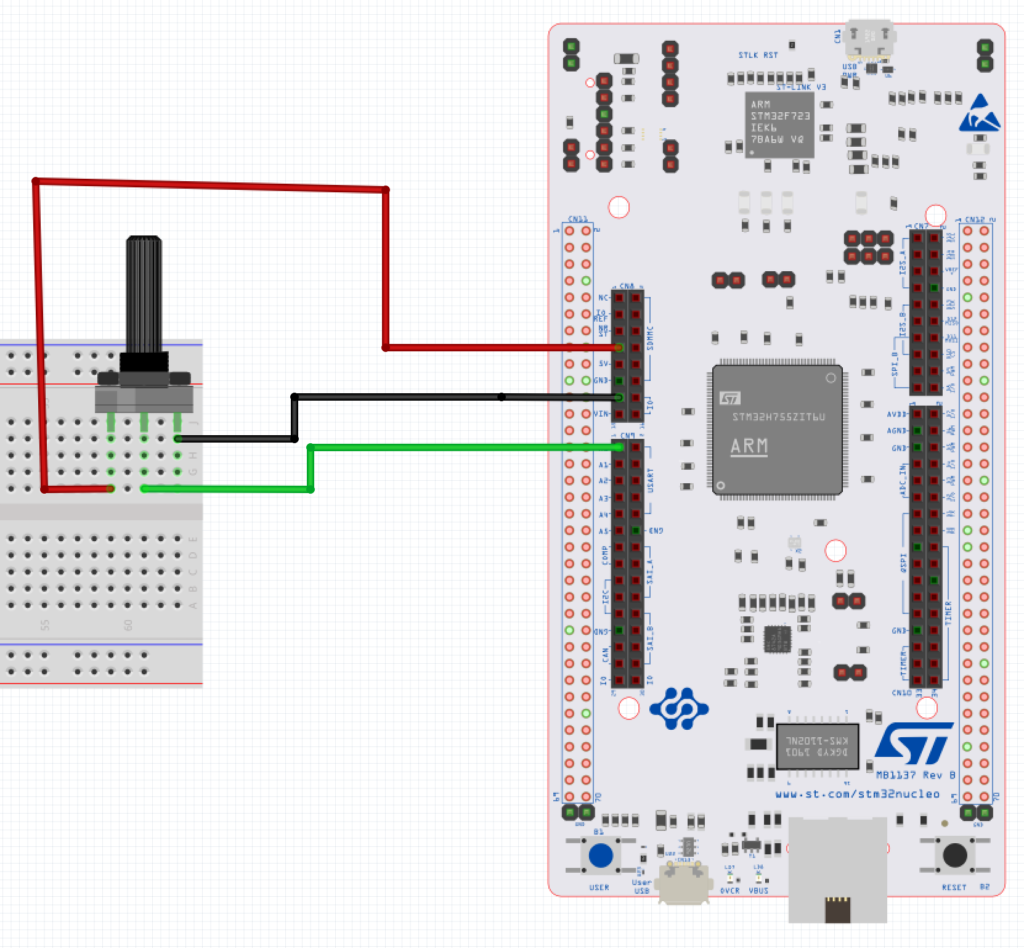
The connection is as following:
- Right leg of the pot to 3V3
- Middle leg to A0 of Arduino connection (PA3)
- Left leg to GND
4. Code
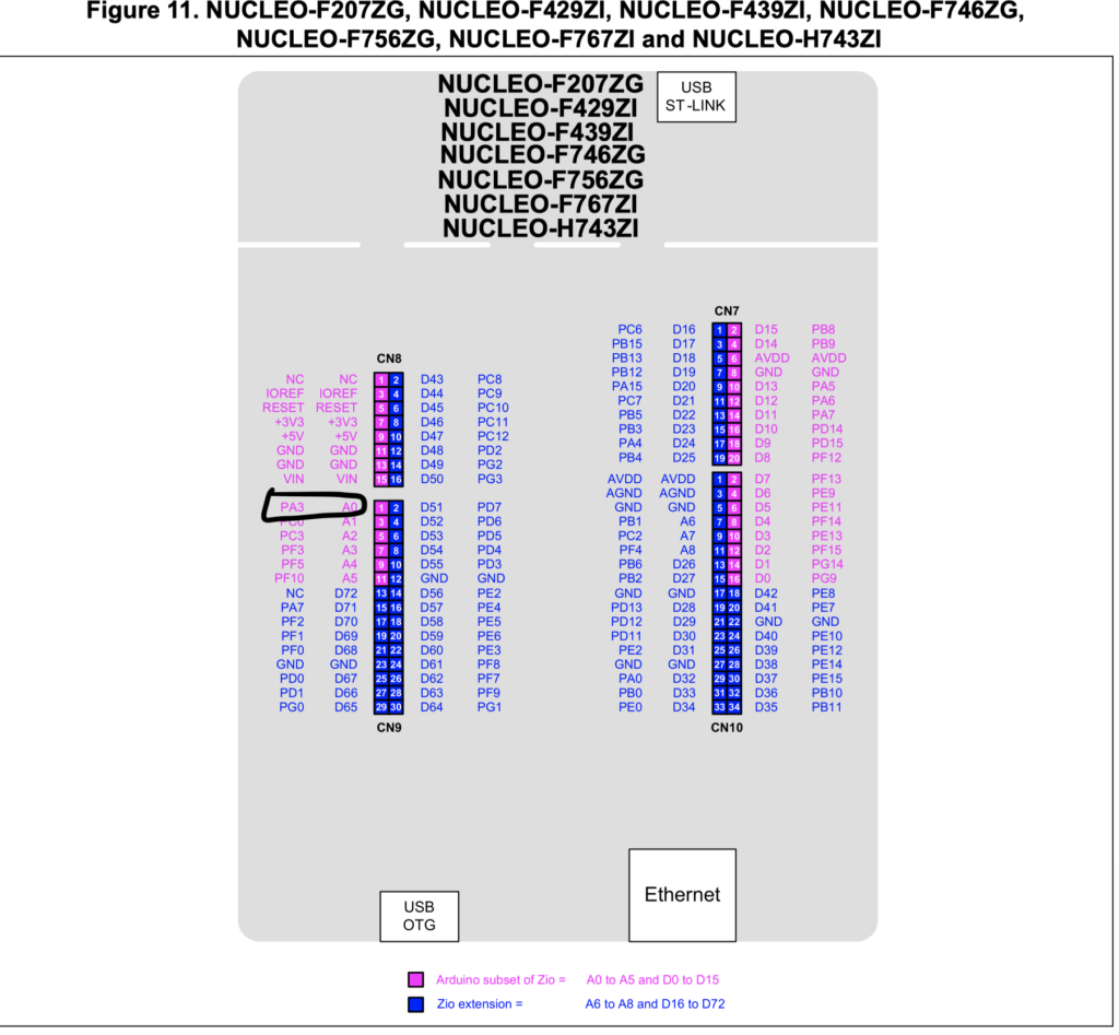
Before we start, we need to get the actual pin of Arduino A0. From Nucleo-144 User Manual, Arduino A0 is connected to PA3.
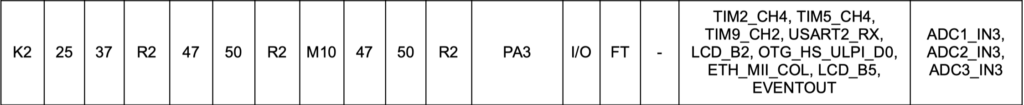
Now, we need to know which channel of ADC is connected to PA3. From the datasheet, PA3 is connected to ADC1_CH3.
After that we can start configuring our pin and ADC.
We start off by Enabling Clock access to GPIOA.
Since the GPIOA is connected to AHB1 bus as shown in figure below
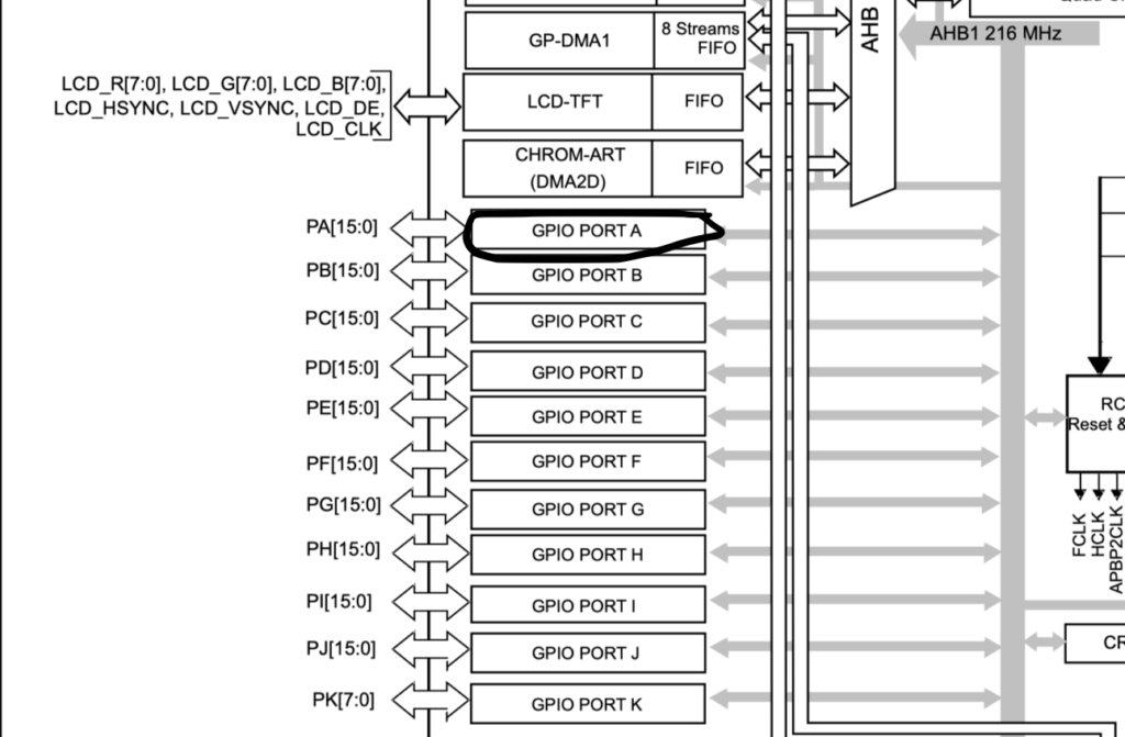
Hence we can enable clock access to GPIOA as following
RCC->AHB1ENR|=RCC_AHB1ENR_GPIOAEN;
Since ADC is connected to APB2, we can enable clock access to ADC1 as following:
RCC->APB2ENR|=RCC_APB2ENR_ADC1EN;
After that we can configure PA3 as analog. From the reference manual, GPIO section, mode register.
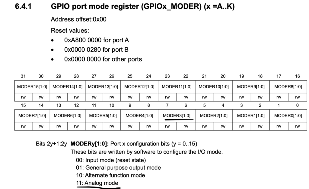
In order to set PA3 as analog, we need to set bit 6 and bit 7 as following
GPIOA->MODER|=GPIO_MODER_MODER3_0|GPIO_MODER_MODER3_1;
Now, we can start configure the ADC module.
We start off by setting the rank of the channel. We need to set PA3 to be first in conversion sequence as following
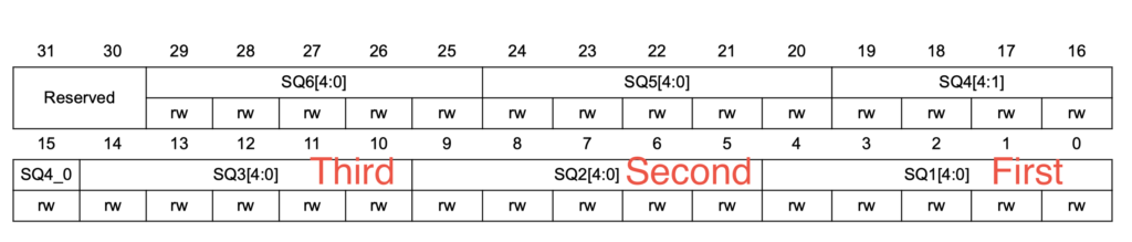
#define CH3 0x03
ADC1->SQR3|=(CH3<<0);
After that we enable the ADC:
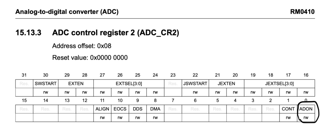
ADC1->CR2|=ADC_CR2_ADON;
In the main loop
We start the conversion:
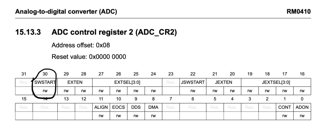
ADC1->CR2|=ADC_CR2_SWSTART;
wait until the conversion is ended
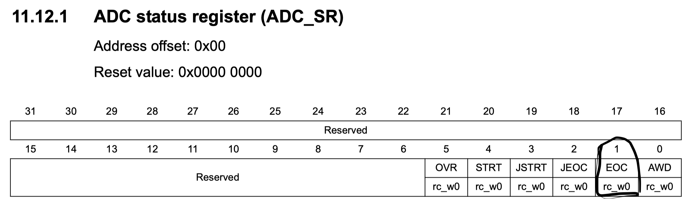
while(((ADC1->SR) & ADC_SR_EOC) == 0);
store the adc data to a variable
adc_data=ADC1->DR;
hence the entire code is as following:
#include "stm32f7xx.h"                  // Device header

#define CH3 0x03

uint16_t adc_data;

int main(void)
	{
	RCC->AHB1ENR|=RCC_AHB1ENR_GPIOAEN;
	RCC->APB2ENR|=RCC_APB2ENR_ADC1EN;

	GPIOA->MODER|=GPIO_MODER_MODER3_0|GPIO_MODER_MODER3_1;
	ADC1->SQR1=0;
	ADC1->SQR3|=(CH3<<0);
	ADC1->CR2|=ADC_CR2_ADON;
	while(1)
		{
		ADC1->CR2|=ADC_CR2_SWSTART;
		while(((ADC1->SR) & ADC_SR_EOC) == 0);
		adc_data=ADC1->DR;
		}


	}
5. Result
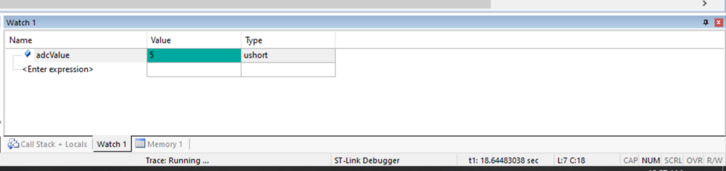
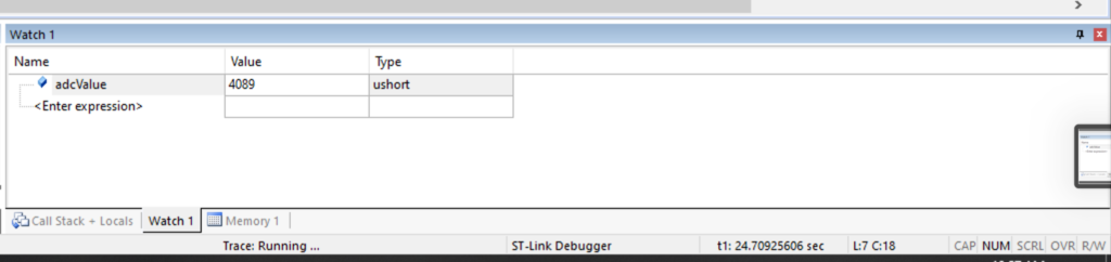
After compiling the code, uploading the code to mcu, opening a debug session in keil uVision
Rotate the potentiometer and observe the adc_data in watch window
Happy coding 🙂
Add Comment