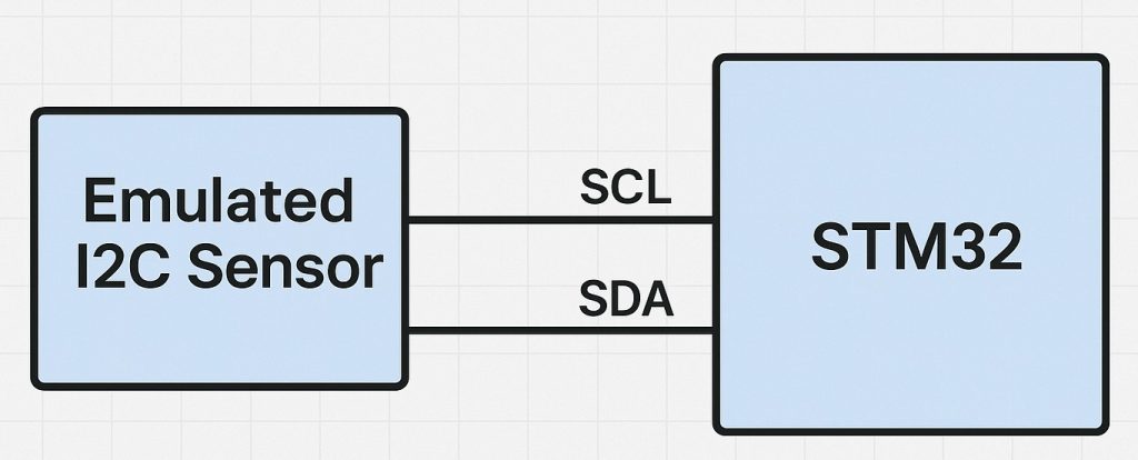
In this part of the guide, we will extend the emulated sensor by introducing control over the rate of its internal ADC conversions. By adjusting this rate, the slave STM32 can mimic real-world sensors that allow the master to configure sampling frequency, enabling more realistic testing and system validation.
In this guide, we shall cover the following:
- Why this is important.
- Slave configuration.
- Slave firmware.
- Master firmware.
- Results.
1. Why this is Important:
1.1. Mimicking Real Sensor Timing
Real sensors often use internal clocking or timers to schedule ADC conversions at fixed intervals. By using an STM32 timer to control when new ADC values are generated, the emulated sensor reproduces this exact timing behavior, ensuring the master only sees fresh data at the expected rate.
1.2. Preventing Unrealistic Data Updates
Without timer control, the slave could update its ADC values every time the master requests them, which is not how real devices work. A timer enforces proper pacing, so the master cannot poll faster than the sensor can realistically respond.
1.3. Power and Performance Modeling
In actual sensors, slower timer-driven sampling reduces power consumption, while faster timers increase responsiveness. By tying the conversion rate to a timer, the emulator can simulate both low-power and high-performance modes, which is vital for system-level power and performance testing.
1.4. Synchronization with Master Requests
The master device may expect new data only after a fixed conversion interval. A timer ensures that new ADC values are generated consistently and predictably, preventing synchronization issues, buffer overruns, or stale data being read repeatedly.
1.5. Configurable Test Scenarios
Since timers on STM32 can be dynamically configured, the emulator can easily switch between different conversion rates by adjusting timer settings. This allows developers to test how the master behaves under different sensor modes (e.g., 1 Hz, 10 Hz, or 1 kHz sampling).
1.6. Data Integrity Validation
By generating ADC values strictly on timer events, it becomes easier to guarantee that data integrity is preserved—one fresh sample per timer period. This aligns with how real sensors guarantee a stable and predictable data flow.
In summary:
Using a timer to control ADC conversion rate in the emulated slave makes the behavior much closer to a real-world sensor. It ensures accurate timing, prevents unrealistic data availability, and provides a flexible way to simulate different operating modes for reliable system testing.
| Aspect | Why It Matters |
|---|---|
| Mimicking Real Sensors | Real sensors rely on internal clocks/timers to schedule ADC conversions; using STM32 timer makes the emulation realistic. |
| Preventing Unrealistic Updates | Stops the slave from generating new data on every master request, ensuring pacing matches real hardware. |
| Power & Performance Modeling | Timer-driven sampling allows simulating low-power slow modes vs. high-performance fast modes. |
| Master Synchronization | Ensures fresh data is only available at predictable intervals, preventing buffer overruns or stale reads. |
| Configurable Scenarios | Timer settings can be changed to test different sensor operating frequencies (e.g., 1 Hz, 10 Hz, 1 kHz). |
| Data Integrity | Guarantees exactly one new sample per timer tick, avoiding inconsistent or duplicate data. |
2. Slave Configuration:
Open the slave .ioc file from project explorer. Once the i.oc opened, STM32CubeMX configuration tool will appear.
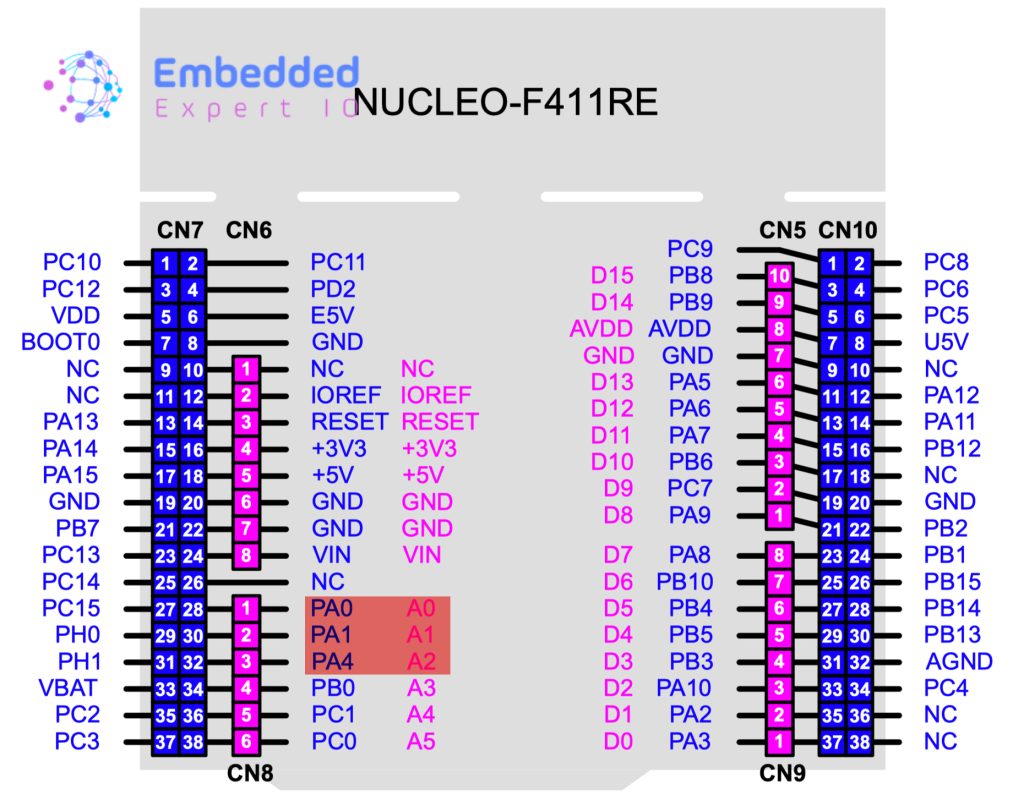
From Analog, select ADC1 and enable IN0, IN1 and IN4.
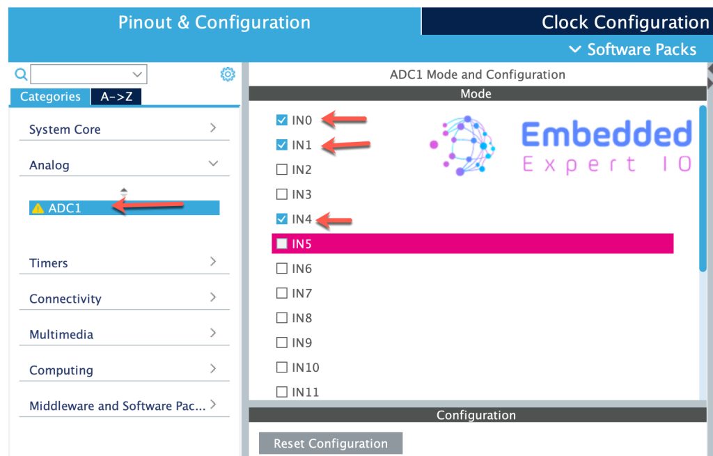
These pins are PA0, PA1 and PA4 respectively. These pins are A0, A1 and A2 of Arduino pin headers.
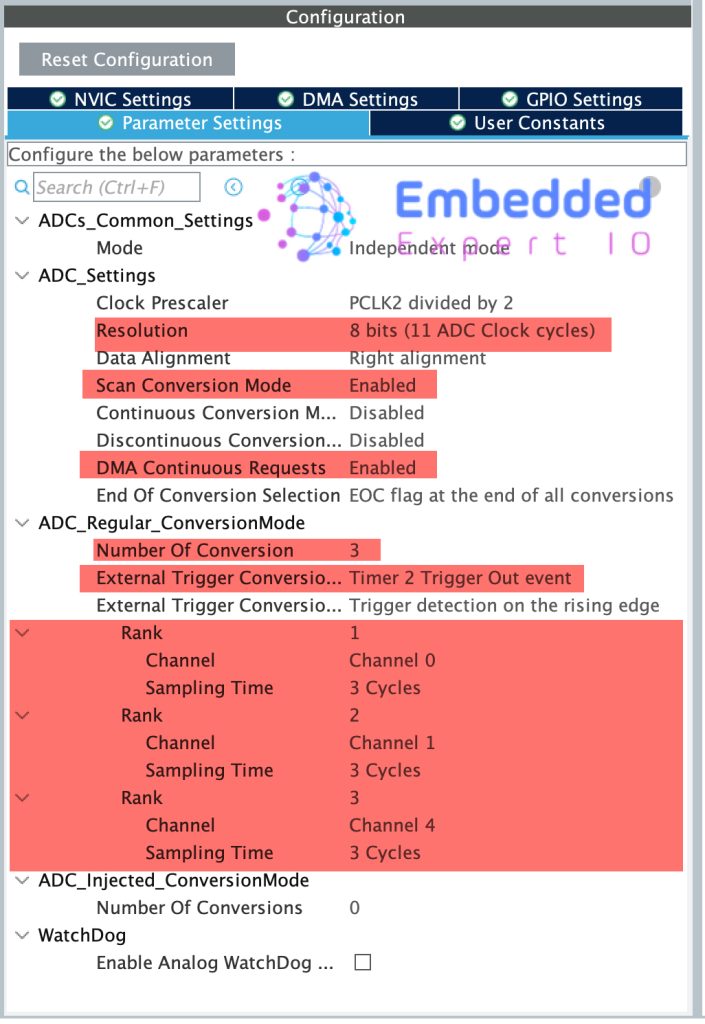
Next, configure the ADC as follows:
- Resolution to 8 bit.
- Scan Conversion to Enabled.
- DMA Continuous Requests to Enabled.
- Number of conversions to 3.
- External trigger to Timer 2 trigger out event.
- Rank 1 to CH0, Rank 2 to CH1 and Rank 3 to CH4.
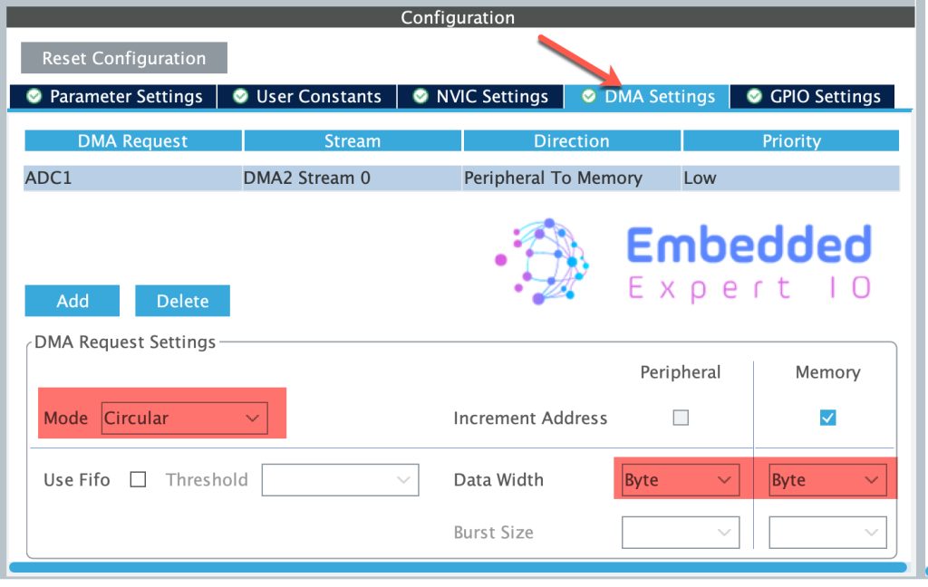
Next, configure the DMA as follows:
- Mode to circular.
- Data width to Byte for Peripheral and Memory.
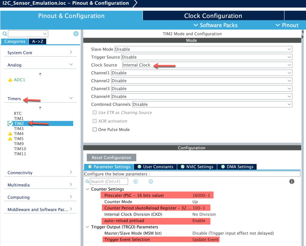
Next, from Timers select TIM2:
Configure it as follows:
- Clock source to internal.
- PSC to 16000-1.
- Counter period to 100-1.
- Auto-reload preload to Enabled.
- Trigger Event selection to Update Event.
Thats all for the slave configuration. Save the project and the project shall be configured.
3. Slave Firmware:
Once the project is configured, main.c will be opened.
In user code begin PV, declare the following array:
uint8_t ADC_Data[3];
This array shall hold the converted ADC data.
We shall nominate ConfigReg1 for rate control
The rate as follows:
- 0 -> 100ms
- 1 -> 50ms
- 2 -> 10ms
#define ConfigReg1 0x00  /*Rate of conversion 0-> 100ms  1->50ms   2-> 10ms*/

#define ConfigReg2 0x01	 /*Interrupt Generation , To be handled later*/

#define ReadReg1 0x03   //Read ADC Data
Next, in HAL_I2C_SlaveRxCpltCallback function, modify the storage for register as follows:
void HAL_I2C_SlaveRxCpltCallback(I2C_HandleTypeDef *hi2c)
{
    if (hi2c->Instance == I2C1)
    {

            CurrentRegister = RegisterData[0]; // first byte = register

            if (CurrentRegister == ConfigReg1)
            {
                switch ( RegisterData[1])
                {
                	case 0: __HAL_TIM_SET_AUTORELOAD(&htim2, 100-1);
                		break;
                	case 1: __HAL_TIM_SET_AUTORELOAD(&htim2, 50-1);
                		break;
                	case 2: __HAL_TIM_SET_AUTORELOAD(&htim2, 10-1);
                		break;
                	default: __HAL_TIM_SET_AUTORELOAD(&htim2, 100-1);
                		break;

                }
            }
            else if (CurrentRegister == ConfigReg2)
            {
                ConfigReg2Value = RegisterData[1];
            }
    }


}
This function is the I²C slave receive complete callback — it runs whenever the STM32 (acting as an I²C slave) successfully receives data from the master. Let’s break it down step by step:
1. Callback condition
if (hi2c->Instance == I2C1)
- Ensures the callback is only executed if the I²C peripheral involved is
I2C1.
2. Decode the received register address
CurrentRegister = RegisterData[0]; // first byte = register
- The first byte sent by the master is treated as a register address (e.g., ConfigReg1, ConfigReg2, etc.).
- This tells the slave which register the master is trying to configure.
3. Handling ConfigReg1
if (CurrentRegister == ConfigReg1)
{
    switch (RegisterData[1])
    {
        case 0: __HAL_TIM_SET_AUTORELOAD(&htim2, 100-1); break;
        case 1: __HAL_TIM_SET_AUTORELOAD(&htim2, 50-1);  break;
        case 2: __HAL_TIM_SET_AUTORELOAD(&htim2, 10-1);  break;
        default: __HAL_TIM_SET_AUTORELOAD(&htim2, 100-1); break;
    }
}
- If the master wrote to
ConfigReg1:- The second byte (
RegisterData[1]) is interpreted as a mode or setting. - Depending on the value (0, 1, 2, or other), the code changes the auto-reload value of
TIM2. __HAL_TIM_SET_AUTORELOADsets the timer’s ARR register, which controls the period of the timer interrupt.- Smaller ARR → faster timer interrupts (higher update rate).
- Larger ARR → slower timer interrupts (lower update rate).
- Example:
case 0→ ARR = 99 → slower ADC sampling.case 2→ ARR = 9 → much faster ADC sampling.
- The second byte (
In other words, ConfigReg1 controls the ADC sampling rate through Timer2.
For the AL_I2C_AddrCallback, when read request happen, transmit the new ADC value
void HAL_I2C_AddrCallback(I2C_HandleTypeDef *hi2c, uint8_t TransferDirection, uint16_t AddrMatchCode)
{

	if(hi2c->Instance==I2C1)
	{

		if(TransferDirection==I2C_DIRECTION_TRANSMIT)
		{

			HAL_I2C_Slave_Seq_Receive_IT(hi2c, RegisterData, 2, I2C_FIRST_FRAME);

		}

		else
		{
            if (RegisterData[0] == ReadReg1)   // <-- prepare fresh data here
            {
                SensorData[0] = ADC_Data[0];
                SensorData[1] = ADC_Data[1];
                SensorData[2] = ADC_Data[2];
            }
			HAL_I2C_Slave_Seq_Transmit_IT(hi2c,SensorData, 3, I2C_FIRST_AND_LAST_FRAME);
		}


	}

}
t runs every time the master addresses your STM32 slave (I2C1) and indicates whether the master wants to write(transmit) or read from the slave.
Let’s go step by step:
1. Make sure it’s the right I²C peripheral
if (hi2c->Instance == I2C1)
- Only handle events for
I2C1.
2. Master → Slave (Write direction)
if (TransferDirection == I2C_DIRECTION_TRANSMIT)
{
    HAL_I2C_Slave_Seq_Receive_IT(hi2c, RegisterData, 2, I2C_FIRST_FRAME);
}
- The master wants to send data to the slave.
- The slave prepares to receive 2 bytes into
RegisterData[]:RegisterData[0]→ register address (e.g., ConfigReg1, ReadReg1, etc.)RegisterData[1]→ value to be written.
- Using
I2C_FIRST_FRAMEmeans this may be part of a longer I²C transaction.
3. Master ← Slave (Read direction)
else
{
    if (RegisterData[0] == ReadReg1)   // <-- prepare fresh data here
    {
        SensorData[0] = ADC_Data[0];
        SensorData[1] = ADC_Data[1];
        SensorData[2] = ADC_Data[2];
    }
    HAL_I2C_Slave_Seq_Transmit_IT(hi2c, SensorData, 3, I2C_FIRST_AND_LAST_FRAME);
}
- The master wants to read from the slave.
- Before sending data, the slave checks if the last register accessed was
ReadReg1:- If yes, it loads fresh ADC values into
SensorData[]. - That way, the master always gets up-to-date sensor data.
- If yes, it loads fresh ADC values into
- Then it starts a non-blocking transmit of 3 bytes (
SensorData[]) back to the master. - The flag
I2C_FIRST_AND_LAST_FRAMEmeans this is both the start and end of the transfer.
Finally, in user code begin 2 in main function:
Simply, start the ADC in DMA mode and start the timer as follows:
  HAL_ADC_Start_DMA(&hadc1, ADC_Data, 3);

  HAL_TIM_Base_Start(&htim2);
Thats all for the slave configuration. Save the project and run it on your MCU as follows:

4. Master Firmware:
In main.c file of the master STM32, in user code begin 2 in main function:
Configure the conversion rate to be 10ms by sending q2 as follows:
  	  SlaveData[0]=0x00;
  	  SlaveData[1]=2;
  	  HAL_I2C_Master_Transmit(&hi2c1, (0x1D<<1), &SlaveData, 2, 100);
In user code begin 3 in while loop:
Read the sensor ADC data as follows:
	  HAL_I2C_Mem_Read(&hi2c1, (0x1D<<1), 0x03, 1, SensorData, 3, 100);
	  HAL_Delay(100);
That all for the master configuration. Save the project and start a debugging session as follows:

5. Results:
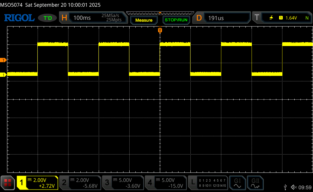
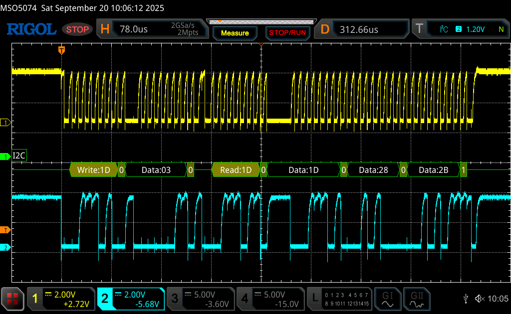
Before sending the conversion rate value, the ADC converts the channels each 100ms:
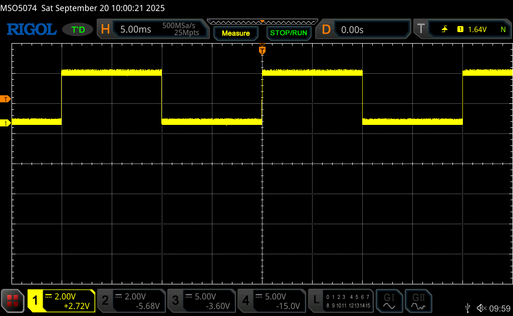
Once the master has transferred the configuration data, the ADC shall convert the channels each 10ms as shown:
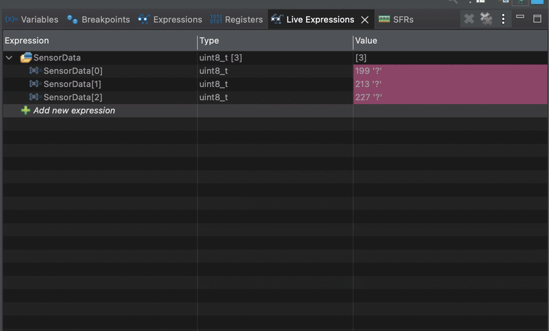
By adding SensorData to Live expressions in the debugging session, you should get 3 ADC as follows:
Here is a sample from the decoded bus:
In next part, we shall introduce interrupt generation to generate high level to inform the master there is new data. Stay tuned.
Happy coding 😉
Add Comment