
In this guide, we shall take a look at the advanced timer of STM32 and it’s features and how to configure it to generate PWM signal with complementary output and later we shall introduce a dead time.
In this guide, we shall cover the following:
- Features of advanced timer in STM32.
- Complementary output.
- Developing the driver.
- Results.
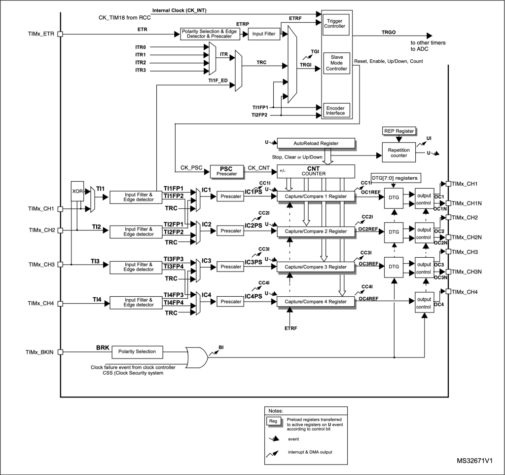
1. Features of Advanced Timer in STM32:
TIM1 timer features include:
• 16-bit up, down, up/down auto-reload counter.
• 16-bit programmable prescaler allowing dividing (also “on the fly”) the counter clock frequency either by any factor between 1 and 65536.
• Up to 4 independent channels for:
– Input Capture
– Output Compare
– PWM generation (Edge and Center-aligned Mode)
– One-pulse mode output
• Complementary outputs with programmable dead-time
• Synchronization circuit to control the timer with external signals and to interconnect several timers together.
• Repetition counter to update the timer registers only after a given number of cycles of the counter.
• Break input to put the timer’s output signals in reset state or in a known state.
• Interrupt/DMA generation on the following events:
– Update: counter overflow/underflow, counter initialization (by software or internal/external trigger)
– Trigger event (counter start, stop, initialization or count by internal/external trigger)
– Input capture
– Output compare
– Break input
• Supports incremental (quadrature) encoder and hall-sensor circuitry for positioning purposes
• Trigger input for external clock or cycle-by-cycle current management.
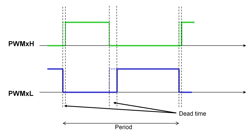
2. Complementary Output:
The complementary output of PWM is a method to generate an inverted signal of the original PWM with dead time. This is typical being used in generating PWM signal for gate drive of MOSFETs, synchronous buck-boost converter etc.
The typical output of PWM and it’s complementary shown in figure below:
3. Developing the Driver:
Before we develop the driver, we need to find which pins are connected to TIM1_CH1 and TIM1_CH1N. We can find these information in the datasheet as following:
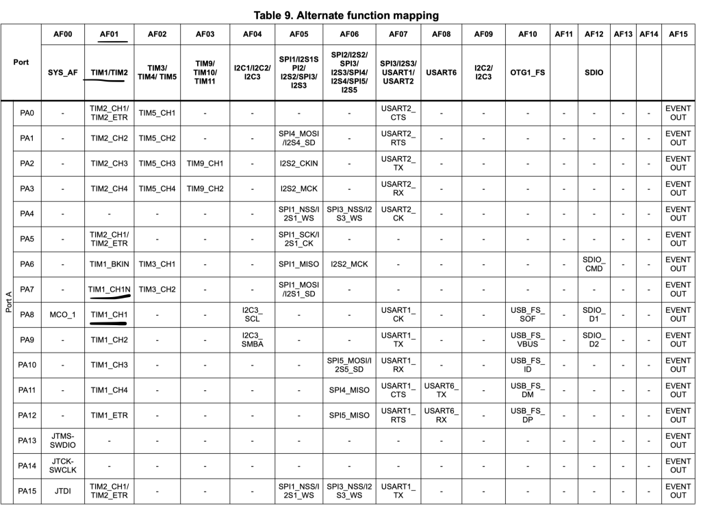
We can find that PA7 and PA8 are for CH1N and CH1 respectively. Also, the alternate function is AF01.
On another hand, we need to find which bus TIM1 is connected to:
This can be also found in the datasheet:
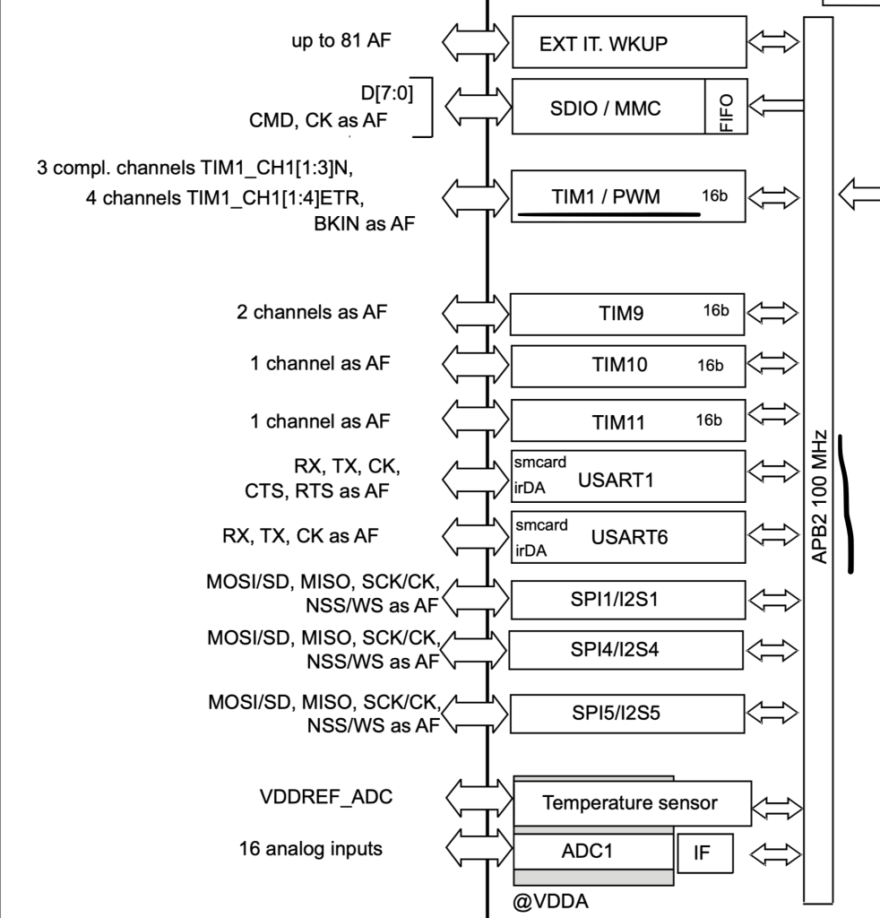
Hence, TIM1 is connected to APB2.
We start off by including the main stm32 header file:
#include "stm32f4xx.h"
Create a symbolic name to hold the alternate function:
#define TIM1AF 0x01
In main function:
Enable clock access to GPIOA:
Check this guide for how to enable clock access to GPIOA and set the alternate function.
int main(void)
{
	/*Enable clock access to GPIOA*/
	RCC->AHB1ENR|=RCC_AHB1ENR_GPIOAEN;
Set PA7 and PA8 to alternate function:
	/*Configure PA7 and PA8 as alternate mode*/
	GPIOA->MODER|=(GPIO_MODER_MODE7_1)|(GPIO_MODER_MODE8_1);
	GPIOA->MODER&=~(GPIO_MODER_MODE7_0)|(GPIO_MODER_MODE8_0);
Select which alternate function to be used:
	/*Select which alternate function*/
	/*Set PA7 to AF01*/
	GPIOA->AFR[0]|=(TIM1AF<<GPIO_AFRL_AFSEL7_Pos);
	/*Set PA8 to AF01*/
	GPIOA->AFR[1]|=(TIM1AF<<GPIO_AFRH_AFSEL8_Pos);
Thats all for GPIO configuration.
Now, timer configuration.
Enable clock access to TIM1:
	/*Enable clock access to TIM1*/
	RCC->APB2ENR|=RCC_APB2ENR_TIM1EN;
Set Prescaler and ARR to 15 and 100 respectively as following:
	/*Set Prescaler to 16-1 to get 1MHz*/
	TIM1->PSC=15;

	/*Set ARR to 1000 to get 1KHz*/

	TIM1->ARR=1000;
This will give us 1KHz PWM signal.
Configure CH1 to be PWM Mode 1 as following:
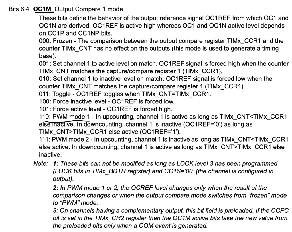
	/*Configure CH1 to be PWM channel*/

	TIM1->CCMR1|=TIM_CCMR1_OC1M_2|TIM_CCMR1_OC1M_1;
Enable channel 1 and the complementary channel:
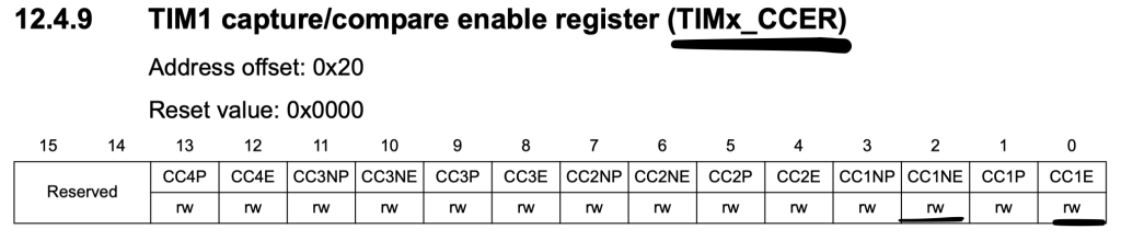
	/*Enable CH1 and CH1 complementary output*/

	TIM1->CCER|=TIM_CCER_CC1E|TIM_CCER_CC1NE;
Enable main output:
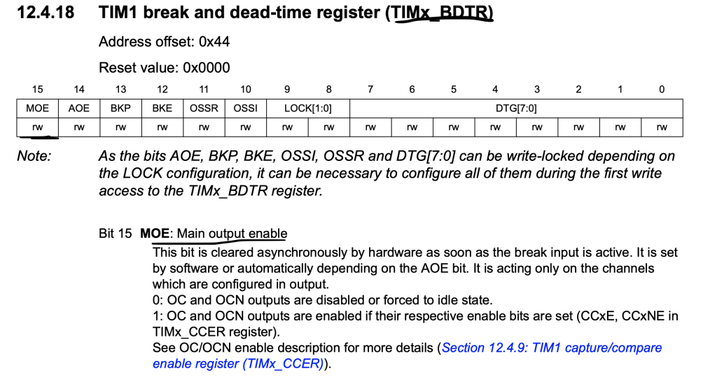
	/*Enable Main output*/

	TIM1->BDTR|=TIM_BDTR_MOE;
Set CCR1 to 500 to generate 50% duty cycle:
	/*Set Duty cycle to be 500 (50%)*/
	TIM1->CCR1=500;
Finally enable the timer:
	/*Enable TIM1*/

	TIM1->CR1|=TIM_CR1_CEN;
Hence, the entire code as following:
#include "stm32f4xx.h"

/*
 * PA7->TIM1_CH1N
 * PA8->TIM1_CH1
 * */

#define TIM1AF	0x01


int main(void)
{
	/*Enable clock access to GPIOA*/
	RCC->AHB1ENR|=RCC_AHB1ENR_GPIOAEN;

	/*Configure PA7 and PA8 as alternate mode*/
	GPIOA->MODER|=(GPIO_MODER_MODE7_1)|(GPIO_MODER_MODE8_1);
	GPIOA->MODER&=~(GPIO_MODER_MODE7_0)|(GPIO_MODER_MODE8_0);

	/*Select which alternate function*/
	/*Set PA7 to AF01*/
	GPIOA->AFR[0]|=(TIM1AF<<GPIO_AFRL_AFSEL7_Pos);
	/*Set PA8 to AF01*/
	GPIOA->AFR[1]|=(TIM1AF<<GPIO_AFRH_AFSEL8_Pos);

	/*Timer configuration*/

	/*Enable clock access to TIM1*/
	RCC->APB2ENR|=RCC_APB2ENR_TIM1EN;

	/*Set Prescaler to 16-1 to get 1MHz*/
	TIM1->PSC=15;

	/*Set ARR to 1000 to get 1KHz*/

	TIM1->ARR=1000;

	/*Configure CH1 to be PWM channel*/

	TIM1->CCMR1|=TIM_CCMR1_OC1M_2|TIM_CCMR1_OC1M_1;

	/*Enable CH1 and CH1 complementary output*/

	TIM1->CCER|=TIM_CCER_CC1E|TIM_CCER_CC1NE;

	/*Enable Main output*/

	TIM1->BDTR|=TIM_BDTR_MOE;

	/*Set Duty cycle to be 500 (50%)*/
	TIM1->CCR1=500;

	/*Enable TIM1*/

	TIM1->CR1|=TIM_CR1_CEN;


	while(1)
	{

	}

}
4. Results:
Using oscilloscope, use should see the following:

Two PWM signal with duty cycle of 50% and it’s complementary output.
13 Comments
Hello my teacher
TIM 1->CCM1|=
TIM_CCMR1_
OC1M_2 |TIM_CCMR1_OC1M_1;
OC1M_2 and
OC1M_1
What do the numbers 1 and 2 symbolize?
5bit and 4bit in CCMR1 do not correspond to these numbers,
I don’t understand.
Hi,
numbers from 0 to 2 represent which bit of OC1M since this part of register is 3-bit wide.
0=4
1=5
2=6
Yeah,
(1<<4) etc
What does the expression mean? Make bit4 logic 1
( 1<<4 )
yes.
0= bit4 no set= Low=0
1=bit5 set = Logic1
2=bit 6 set= Logic 1
Logic 110 = pwm mod1
I understand now
STM32 Gelişmiş Zamanlayıcılar Bölüm 1:
PWM ve Tamamlayıcı Çıkış Oluşturma
Teacher,
will there be a continuation of this section?
For example, producing 3 phase PWM for 3 phase BLDC motors
with advanced timers, it would be very educational, it is a popular topic.
I use google translate, please forgive any translation errors
I wish you a good rest 15/11/2023
Driving BLDC is not an easy task.
You need special MCU like STM32F3, G4 to do it not F4 since they are both designed for mixed signal operation.
Advanced timer can be used to convert DC to three phase AC.
Hey, I want to generate two complementary sine pwms with shoot through (i.e both the pwm should be ON for a particular duration, if a condition is satisfied. Otherwise they should be complementary). My doubt is can I control the duty cycle of the complementary pwm without changing the original one to make both the PWM on.
Hi,
are you trying to drive bldc motor?
Your clear , simple and precise code example (without YouTube kikifax) was a great help for me. I transferred a working conde from TIM2 to TIM1, nothing was working.
The line “TIM1>BDRL |= TIM_BRTR_MOE;” in your example solved the problem. Thank you !!
The guide uses TIM1.
Add Comment