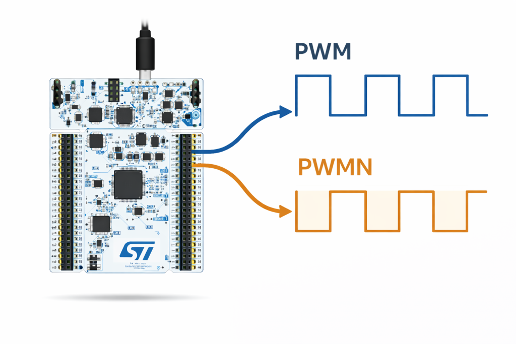
This guide explains how to configure and use TIM1 on STM32F4 to generate precise PWM and complementary PWMN signals with configurable dead-time insertion. It covers the principles of dead-time generation, complementary waveform synchronization, and the practical considerations required for safe and efficient power-stage control.
In this guide, we shall cover the following:
- Why dead time is needed.
- Calculating dead time.
- STM32CubeMX modification.
- Results.
1. Why Dead Time is Needed:
In STM32 microcontrollers, TIM1 is an advanced-control timer capable of generating complementary PWM outputs (PWM and PWMN) with high precision. These signals are widely used to drive half-bridge or full-bridge power stages in applications such as motor control, DC-DC converters, inverters, and industrial power electronics. A fundamental requirement in all these applications is that high-side and low-side switches must never be on simultaneously, as this condition can create a short-circuit path directly across the supply rail. This potentially catastrophic condition is referred to as shoot-through. Even very short overlaps of a few nanoseconds at high voltages or currents can result in MOSFET/IGBT damage, excessive heating, voltage spikes, or electromagnetic interference (EMI).
Dead time is a carefully inserted delay between the switching of complementary outputs that ensures the high-side device turns off completely before the low-side device turns on, and vice versa. TIM1 provides hardware-based dead-time generation, which guarantees precise timing independent of CPU load, interrupts, or software execution delays. This feature is critical because software-based dead-time management is prone to latency, jitter, and timing errors, particularly at high PWM frequencies. Without hardware dead time, even small timing inconsistencies could lead to overlapping conduction, degraded efficiency, thermal stress, and possible device failure.
Key Reasons Dead Time Is Crucial
- Prevention of Shoot-Through:
The primary role of dead time is to eliminate the risk of simultaneous conduction in complementary power devices. By enforcing a minimum delay between the turn-off of one device and the turn-on of the other, shoot-through is avoided, protecting the devices and associated circuitry from catastrophic failure. - Hardware-Enforced Precision:
TIM1 implements dead-time insertion internally using the Dead-Time Generator (DTG) in the BDTR register, allowing sub-microsecond delays at very high PWM frequencies. Hardware enforcement ensures that the delay is deterministic, cycle-accurate, and free from jitter caused by software or interrupt handling, which is essential for stable and reliable operation. - Maintaining Signal Integrity:
Complementary PWM outputs without dead time may overlap or switch too closely, causing voltage spikes and high dv/dt transitions that can stress gate drivers, increase EMI, or generate ringing in power traces. Dead time ensures that PWM and PWMN waveforms are cleanly separated, maintaining waveform integrity for safe switching. - Efficiency and Thermal Management:
By preventing simultaneous conduction, dead time reduces unnecessary power dissipation, ensuring that MOSFETs/IGBTs operate within safe thermal limits. This helps maintain high efficiency in power conversion applications and prolongs the lifetime of components. - Consistent Operation at High PWM Frequencies:
As PWM frequency increases, the time available for switching decreases. Hardware dead time allows precise insertion of necessary delays even at high frequencies (tens or hundreds of kHz), where software-based control would struggle to maintain timing accuracy. - Support for Safe Advanced Control Features:
Dead time is essential when using additional TIM1 features such as break inputs, complementary outputs with polarity control, or synchronized multi-phase PWM. It ensures safe operation under all fault conditions and prevents inadvertent shoot-through when the timer dynamically changes duty cycles or phase alignment.
2. Dead Time Calculation:
Dead Time Calculation
For STM32F4 timers:
- The dead‑time generator uses a dead‑time clock (typically the APB2 timer clock, often 2× PCLK2).
- Dead time is expressed in timer ticks based on the clock frequency.
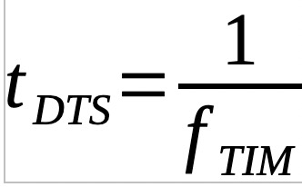
To compute the dead‑time value (DTG register value):
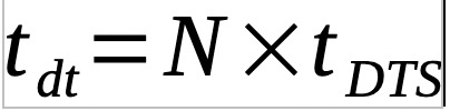
Where:
- Tdts is the dead‑time clock period (inverse of timer clock frequency)
- N is the integer count configured in the BDTR.DTG field
Example:
If the timer clock is 16 MHz, and we want 500 ns of dead time:
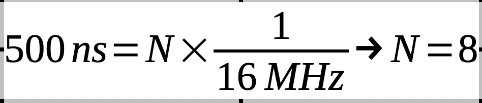
Thus, set DTG = 8 to approximate a 500 ns dead‑time delay.
3. STM32CubeMX Modification:
We shall continue from here.
Open the project using STM32CubeMX.
Once the project has been opened:
In Parameters Settings of TIM1, set the dead time to 8 and click on generate project as follows:

4. Results:
Once you opened the project using STM32CubeIDE, run the project as follows:

BAfter building and flashing the firmware:
Run the application.
Connect a logic analyzer or oscilloscope to the PWM output pins (e.g., PA7 for PWM, PA8 for PWMN).
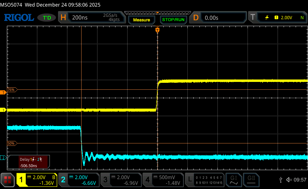
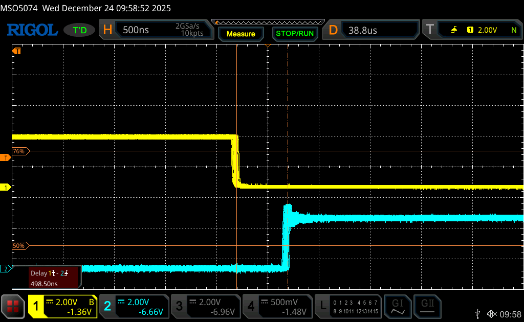
You should observe:
- Two complementary PWM signals
- A clean dead‑time gap between transitions
- ~500 ns delay between turn‑off and turn‑on edges
This confirms that the hardware dead‑time generator is functioning as expected and ensures safe switching transitions.
Happy coding 😉
Add Comment