In this part of the STM32 ADC series, we delve into the concept of sample time and its critical role in determining ADC accuracy and performance. Sample time directly affects how long the ADC samples the input voltage before conversion, influencing both conversion speed and the ability to accurately capture signals—especially those with high source impedance.
In this guide, we shall cover the following:
- Introduction.
- How to calculate sample time for each channel.
- Firmware development.
- Sample time calculation and results.
1. Introduction:
Understanding ADC Sample Time and Its Importance in STM32
The Analog-to-Digital Converter (ADC) in STM32 microcontrollers plays a vital role in bridging the analog and digital worlds by digitizing real-world signals—like temperature, voltage, or sensor readings—into binary values the microcontroller can process. Among the various configurable parameters of the ADC, one of the most fundamental and sometimes overlooked is the sample time.
Sample time defines the duration during which the ADC’s internal capacitor is connected to the external analog signal before the actual digital conversion begins. This phase allows the ADC’s internal sample-and-hold circuit to charge to the analog input voltage. It is expressed in ADC clock cycles and can range from very short (e.g. 1.5 cycles) to significantly longer durations (e.g. 601.5 cycles), depending on the STM32 family and configuration.
Why Sample Time Matters
Sample time has a direct influence on both the accuracy and speed of ADC conversions. The analog input signal must be sampled long enough to allow the internal capacitor to settle to the correct voltage with sufficient precision. If this time is too short, especially for high-impedance sources or slowly changing signals, the voltage captured may not accurately reflect the true input, leading to conversion errors or noisy readings.
Conversely, using a sample time longer than necessary slows down the conversion rate and reduces the maximum number of samples per second, which is critical in high-speed applications like audio or waveform analysis.
Thus, choosing the right sample time is a trade-off:
- Too short: inaccurate results due to insufficient charge time or voltage settling.
- Too long: reduced throughput and slower system response.
What Influences the Required Sample Time?
Several factors influence how much sample time is needed for accurate ADC operation:
- Source Impedance (R<sub>source</sub>):
If the analog signal comes from a high-impedance source—such as a resistive divider, a sensor with weak output, or through filtering resistors—it takes longer for the ADC input to charge to the correct voltage. Higher source impedance → longer required sample time. - ADC Input Capacitance and Internal Resistance:
The STM32 ADC has an internal sample-and-hold circuit with a small capacitor (a few pF) and internal switch resistance. The time constant formed by the source resistance and ADC input affects how quickly the voltage settles. - Accuracy Requirements:
For 12-bit resolution or higher, the sampled voltage needs to settle within a small error margin (e.g., 1/4096 of full scale for 12-bit), which translates into a longer settling time for accurate readings. - ADC Clock Frequency:
Since the sample time is measured in ADC clock cycles, a faster ADC clock shortens the actual time represented by each cycle. This means that for a given settling requirement, you may need to increase the number of cycles if the ADC clock is fast. - Presence of Analog Buffers or Op-Amps:
Buffering the input signal with a low-output-impedance op-amp allows faster charging of the ADC capacitor and permits shorter sample times even for slow or high-impedance sources.
Consequences of Incorrect Sample Time
- Undersampling: If the sample time is too short, the ADC may not capture the correct voltage, leading to conversion errors, voltage droop, or oscillating results.
- Increased Noise: Fast sampling on high-impedance sources can amplify analog noise, making the digital values unstable or incorrect.
- Throughput Bottleneck: Overestimating the required sample time reduces the ADC’s maximum sampling rate, limiting the performance of real-time data acquisition.
- Power Trade-offs: Longer sample times may mean the system stays active longer during each sampling cycle, slightly increasing power consumption—though this is usually minimal.
The Balancing Act
Choosing the optimal sample time is an exercise in balancing:
- Signal integrity (accuracy, stability),
- System requirements (speed, responsiveness),
- Analog characteristics (source impedance, signal frequency),
- and microcontroller limits (clock configuration, resolution, performance).
STM32’s flexibility in offering a range of selectable sample times gives developers control over this trade-off. However, proper understanding is necessary to make informed decisions—especially in precision-sensitive applications like instrumentation, sensor interfaces, or motor control.
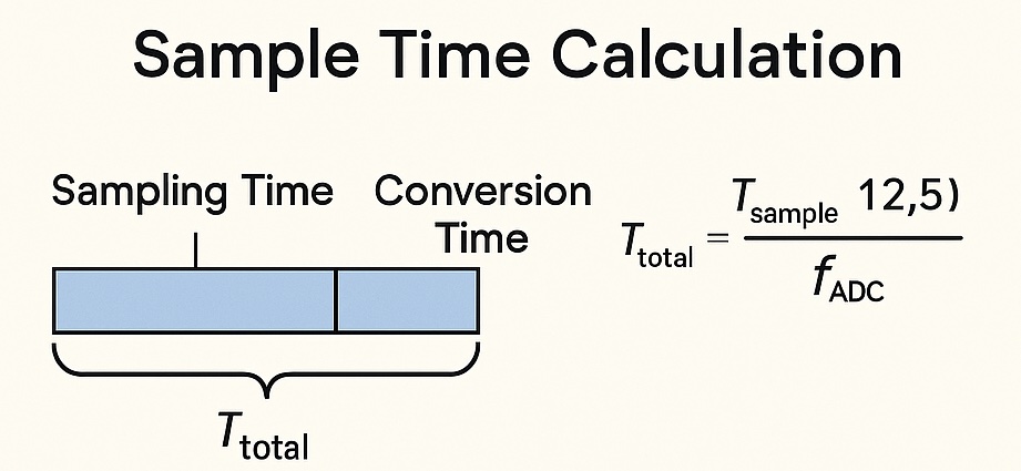
2. Sample Time Calculation:
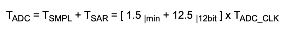
In STM32F4, the ADC conversion time consists of two phases:
- Sampling Time (Ts):
The time during which the ADC samples the input voltage via its sample-and-hold capacitor. You can configure this in STM32CubeMX or directly in theADC_SAMPLETIMEregister. - Conversion Time (Tc):
The time it takes the ADC to convert the sampled analog signal to a digital value. For 12-bit resolution, this is a fixed 12.5 ADC clock cycles.
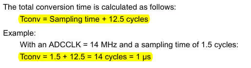
The function to calculate the sampling time as follows:
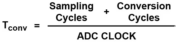
The above formula has 3 parameters:
- Sampling Cycles is the time in terms of ADC CYCLES, taken by a particular channel to sample the data. This parameter is configurable in the cubeMX and it can be configured separately for each channel.
- @Conversion Cycles is the time in terms of ADC CYCLES, taken by the ADC to convert the sampled data. This parameter is not configurable, but it depends on the ADC resolution we set in the cubeMX. The Higher the resolution, the higher will be this parameter. This parameter also varies across different MCUs, but we can find the value in the reference manual of the MCU itself.
- @ADC Clock is the clock at which the ADC is running.
For example the ADC in 12-bit mode in STM32F4 needs 12 cycles and number of cycles for the channel is 3 and ADC clock is 10MHz.
From the equation:
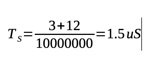
Hence, the ADC shall take 1.5uS to finish the conversion of the channel.
3. Firmware Development:
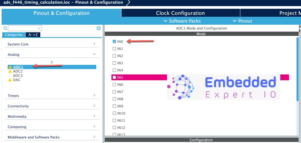
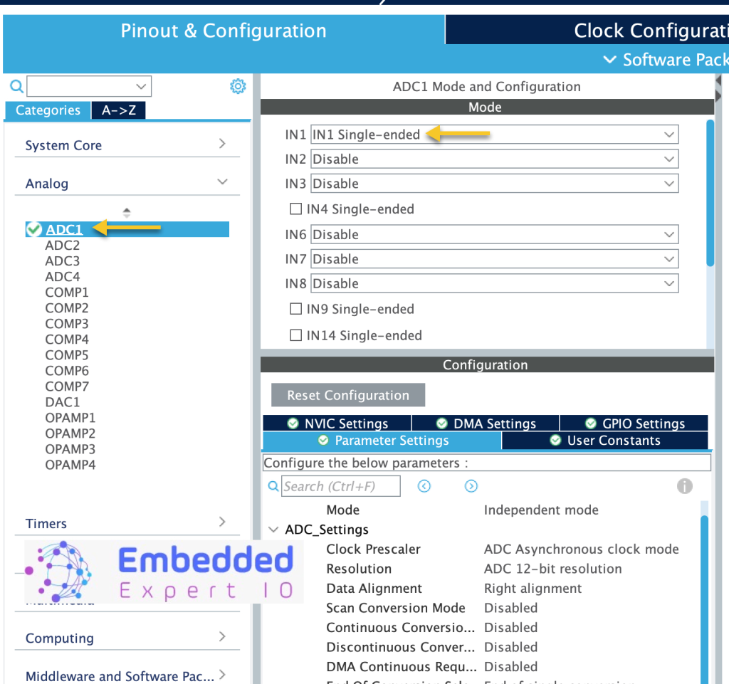
Once you started a new project, enable ADC CH1 as follows:
STM32F4xx series:
STM32F303:
Enable Channel 1 as single Ended
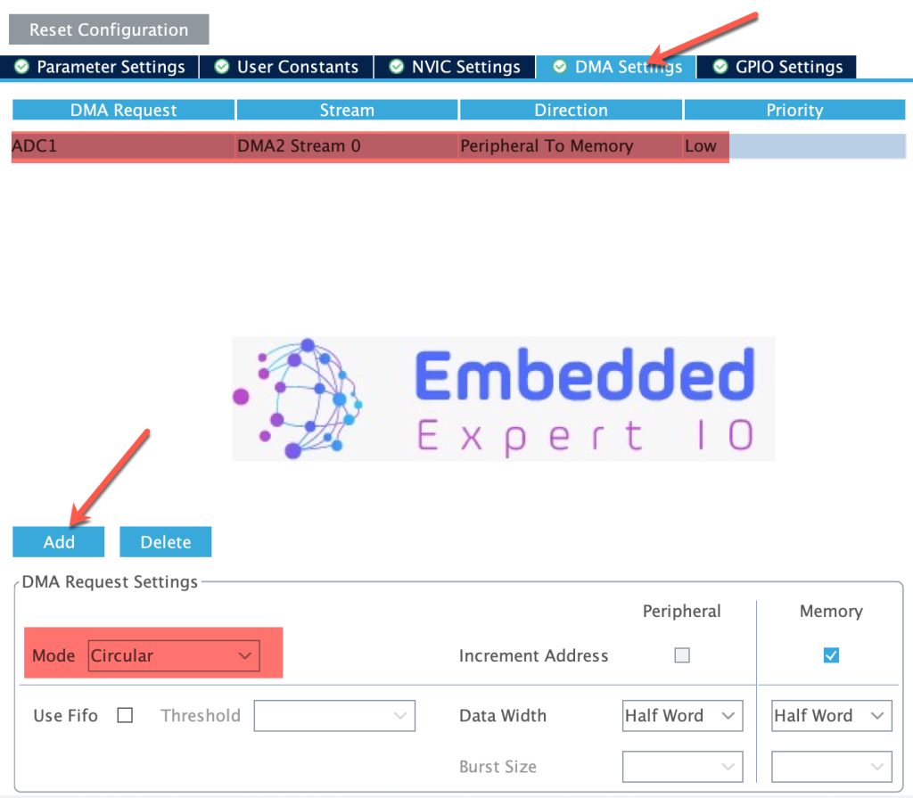
Enable DMA for ADC1 as follows:
Make sure to enable circular mode.
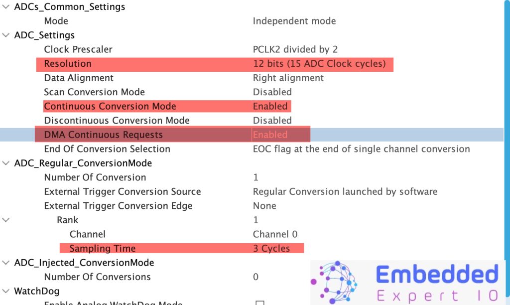
Enable Continuous Conversion Mode and DMA Continuous Request as follows and also make sure that the ADC resolution is 12 bit, Clock prescaler PCLK2 divided by 2.
STM32F4xx:
STM32F303:
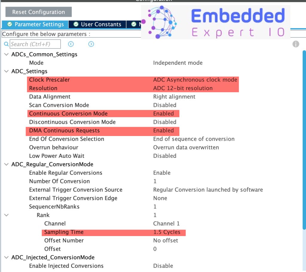
- Set mode to independent.
- Clock Prescaler to ADC Asynchronous Clock Mode.
- Continuous Conversion mde to enabled
- DMA Continuous Request to enabled.
- Set Sampling time to 1.5 cycles.
To get the ADC Clock:
From Clock configuration, we can find the ADC clock as follows:
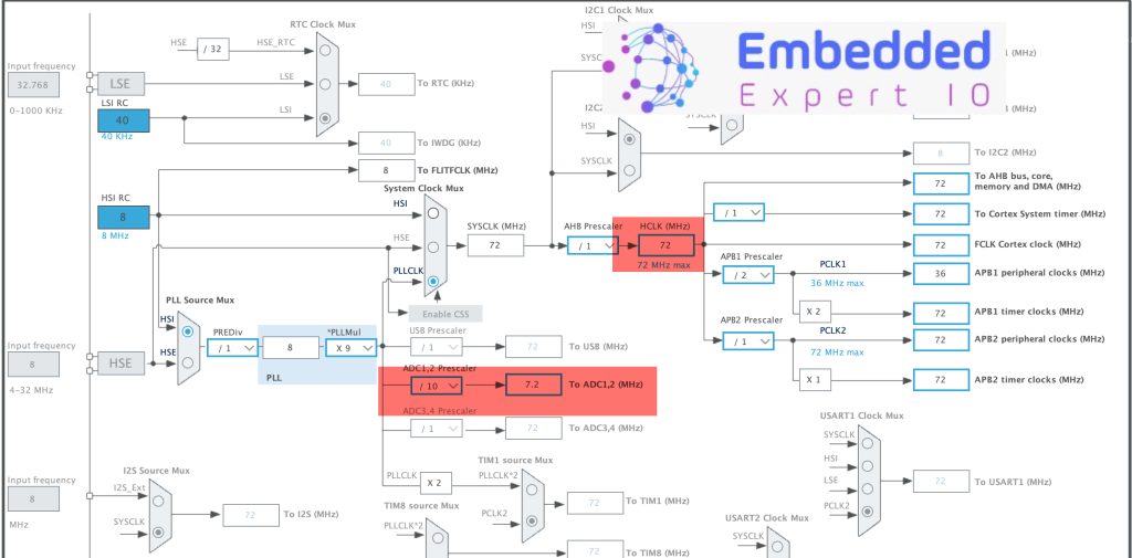
In case there is no dedicated ADC clock, we need to refer to the datasheet of the MCU, in this case, STM32F446RE and check which bus is the ADC clocked from:
The 3 ADC are clocked from APB2 bus, from Clock Configuration within STM32CubeMX, we can find that APB2 clock is 16MHz, hence the ADC clock is 16MHz.
That all for the configuration, save the project and this will generate the code.
For STM32F4 and STM32F303:
In user code begin PV:
#define size 100
uint16_t adcData[size];
User code begin 0:
void HAL_ADC_ConvCpltCallback(ADC_HandleTypeDef* hadc)
{
	HAL_GPIO_TogglePin(GPIOA, GPIO_PIN_5);
}
Start the ADC in DMA as follows:
HAL_ADC_Start_DMA(&hadc1, (uint32_t*)adcData, size);
4. Sample Time Calculation and Results:
STM32F4:
Since the ADC clock is 16MHz and it is divided by 2:
From the reference manual:
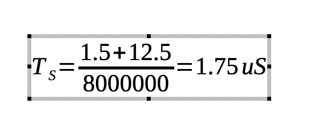
Since we are sampling the ADC 100 times before the DMA trigger and interrupt, we shall get 175uS toggle rate as follows:
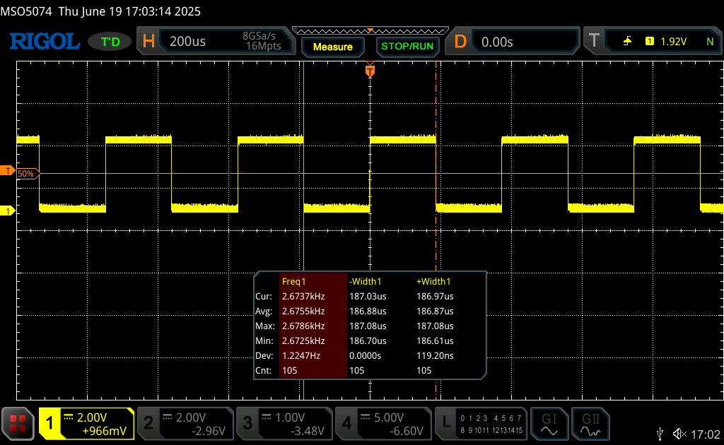
We are getting 187uS which is due to interrupt overhead and HAL latency. The results are near the calculated value multiplied by 100 due to sampling 100 times.
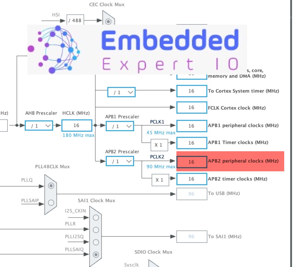
For STM32F303:
Since the clock of the ADC 7.2MHz which we got it from Clock Configuration within CubeMX
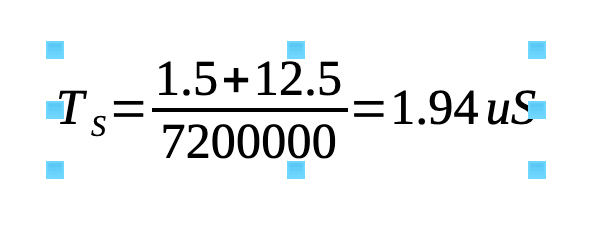
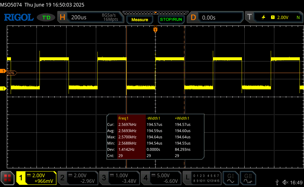
Since we are sampling 100 samples, we are getting 194.7uS which is the same as theoretical one multiplied by 100.
Next, we shall control the behaviour of the ADC using timers.
Stay tuned.
Happy coding 😉
Add Comment