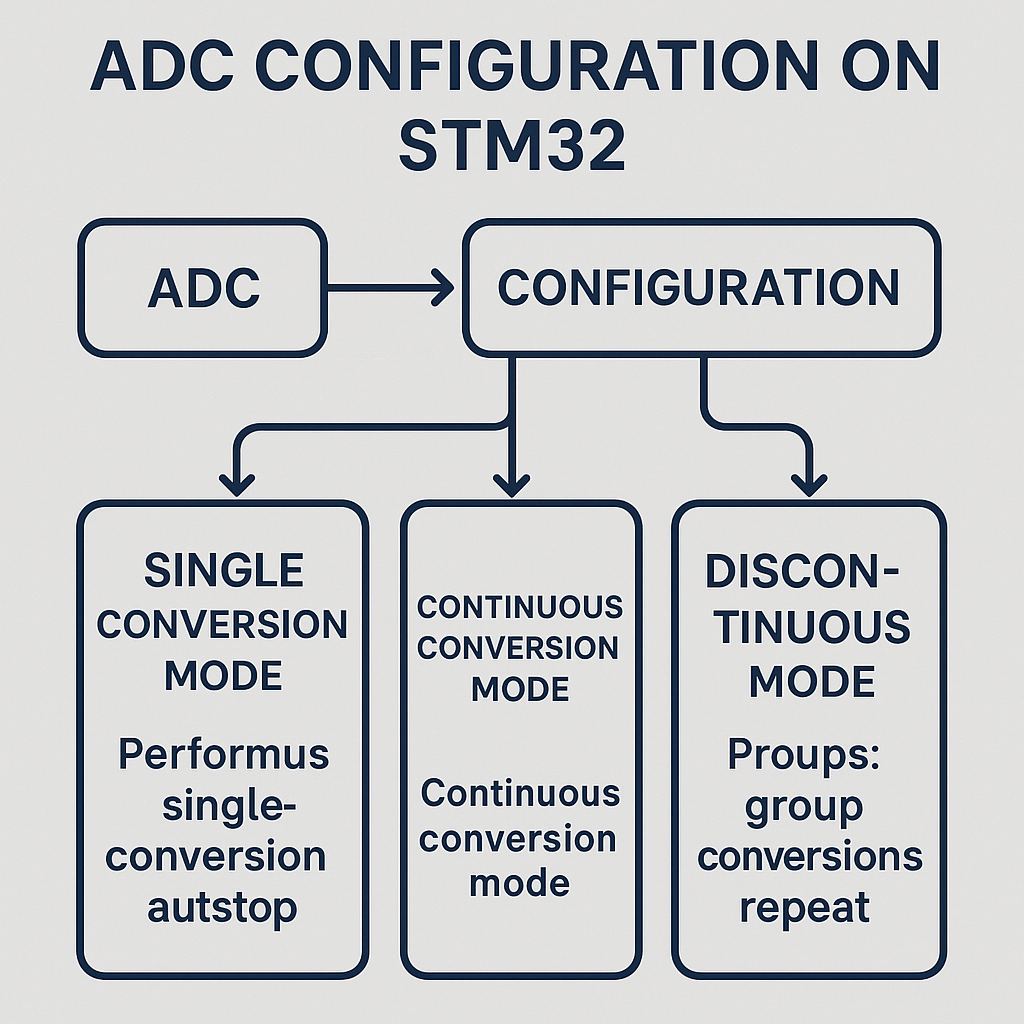
Analog-to-Digital Converters (ADC) on STM32 microcontrollers allow precise measurement of analog signals by converting them into digital values for processing. Understanding the different ADC operating modes—such as single, continuous, and discontinuous—is essential for tailoring performance to specific application needs. In part 1, we shall cover the single Conversion Mode
In this guide, we shall cover the following:
- Introduction to ADC.
- ADC configuration.
- ADC firmware.
- Connection.
- Results.
1. Introduction to ADC:
1.1 What is the ADC
In electronics, an analog-to-digital converter (ADC, A/D, or A-to-D) is a system that converts an analog signal, such as a sound picked up by a microphone or light entering a digital camera, into a digital signal that can be read by STM32.
ADCs can vary greatly between microcontroller. The ADC on the STM32F411 is a 12-bit ADC meaning it has the ability to detect 4096(2^12) discrete analog levels (which is also called Resolution). Some microcontrollers have 8-bit ADCs (2^8 = 256 discrete levels) and some have 16-bit ADCs (2^16 = 65,536 discrete levels).
The way an ADC works is fairly complex. There are a few different ways to achieve this feat (see Wikipedia for a list), but one of the most common technique uses the analog voltage to charge up an internal capacitor and then measure the time it takes to discharge across an internal resistor. The microcontroller monitors the number of clock cycles that pass before the capacitor is discharged. This number of cycles is the number that is returned once the ADC is complete. Other methods used called Successive-approximation ADC which you can read about it in details from this wikipedia page (Link)
For more information about how the adc of STM32F4 works, refer to the user manual (RM0383).
1.2 Relating ADC Value to Voltage
The ADC reports a ratio metric value. This means that the ADC assumes 3.3V is 4095 and anything less than 3.3V will be a ratio between 3.3V and 4095.
For example if the sensor has output voltage of 1.66V hence the ADC output will be (4095/3.3)*1.66=2059.
2. ADC Configuration:
Create new project and name it as ADC_Polling, STM32CubeMX window shall appear.
In analog from left side, select ADC1 and enable IN1 as single ended as following:
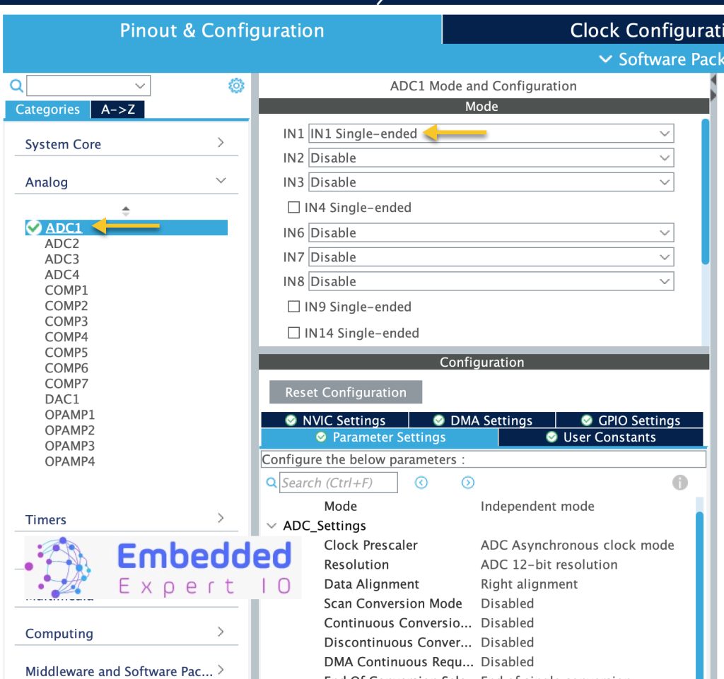
This will enable PA0 as ADC1_IN1.
From parameter settings:
ADC_Settings
- Mode: Independent mode
The ADC operates independently, not synchronized with another ADC unit (STM32F3 has multiple ADCs that can be run in dual mode). - Clock Prescaler: ADC Asynchronous clock mode
The ADC uses an asynchronous clock source, independent of the main APB clock, often for better precision and flexibility. - Resolution: ADC 12-bit resolution
The ADC provides 12-bit digital output, meaning the analog input is quantized into 4096 levels (2¹²). - Data Alignment: Right alignment
The digital conversion result is aligned to the right in the 16-bit ADC data register (least significant bits occupied). This will make handling the data easier. - Scan Conversion Mode: Disabled
Only one channel will be converted; multi-channel scanning is not used. - Continuous Conversion Mode: Disabled
The ADC performs only one conversion when triggered; does not keep converting continuously. - Discontinuous Conversion Mode: Disabled
Not applicable here since scanning is disabled. In scan mode, this would group conversions into smaller sequences. - DMA Continuous Requests: Disabled
DMA is not used to transfer ADC results. Normally used to offload CPU when many conversions are happening. - End Of Conversion Selection: End of single conversion
The End of Conversion (EOC) flag is set after a single conversion (useful for polling or interrupt triggering). - Overrun Behavior: Overrun data overwritten
If a new conversion finishes before the previous data was read, the old data is overwritten. - Low Power Auto Wait: Disabled
The ADC does not wait until the previous data is read before starting a new conversion (can save power in low power mode).
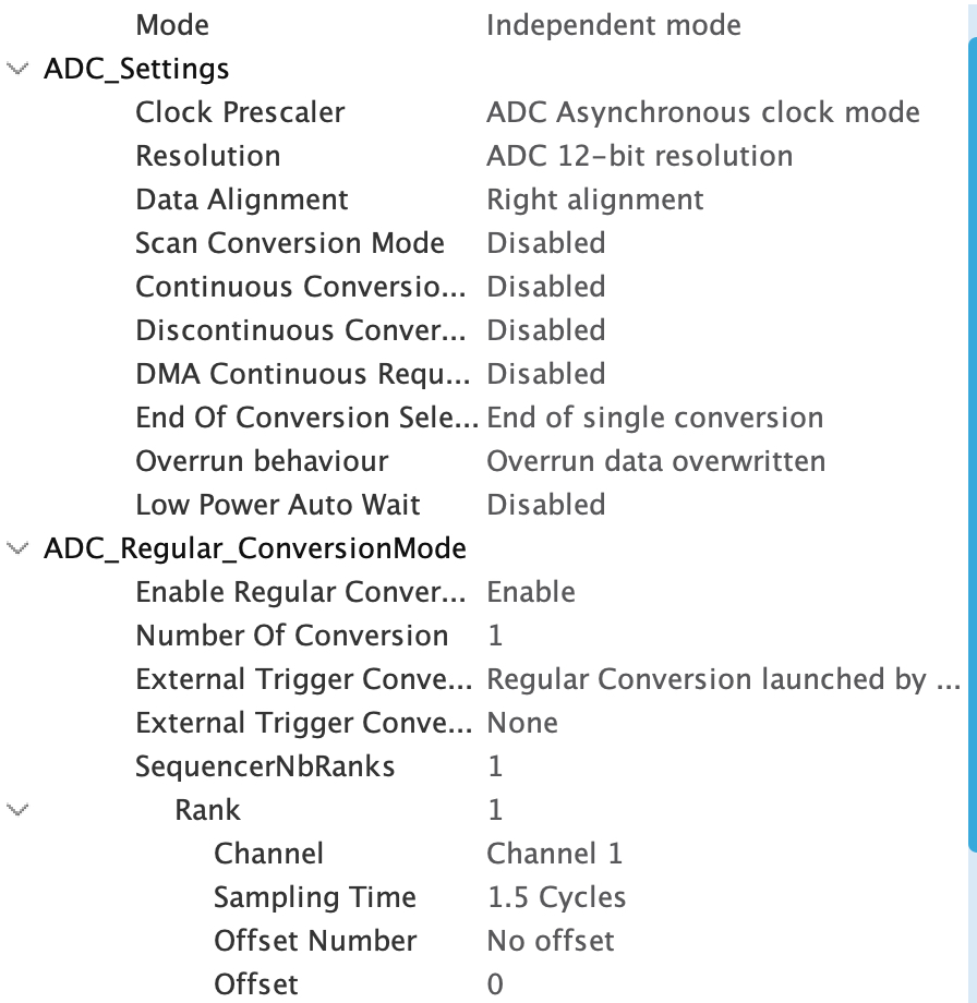
ADC_Regular_ConversionMode
- Enable Regular Conversion: Enable
The regular channel conversion (as opposed to injected conversions) is active. - Number Of Conversion: 1
Only one channel is configured in the regular group (simple case). - External Trigger Conversion: Regular Conversion launched by …
(The rest is truncated, but likely “software” or “timer”)
Determines how the ADC is triggered—probably via software in this case. - External Trigger Conversion Edge: None
No edge detection is enabled for an external trigger—probably meaning software triggering is used. - SequencerNbRanks: 1
Only one rank (position in sequence) is defined in the conversion sequence.
Channel Configuration
- Channel: Channel 1
The ADC is set to convert analog input on ADC Channel 1 (check pin mapping for which GPIO this corresponds to). - Sampling Time: 1.5 Cycles
The ADC samples the input signal for 1.5 ADC clock cycles before converting—faster but less accurate with high-impedance sources. - Offset Number: No offset
No hardware offset correction applied to the measured value. - Offset: 0
The offset value is 0—so the raw ADC value is used directly.
Later in next guides, we shall have deeper look into these configuration and how to use them.
Save the project this will generate the project.
3. ADC Firmware Development:
After the project has been generated, main.c shall be opened.
After the project has been generated, main.c shall be opened.
In main.c, in user code begin PV, declare a variable to hold the ADC results as following:
uint16_t adcValue;
n while 1 loop in user code begin 3, we shall the ADC as following:
HAL_ADC_Start(&hadc1);
The HAL_ADC_Start will start the ADC conversion and take one parameter which is the ADC handle which is hadc1 in this case.
Next, we shall wait for the ADC to finish conversion by polling the ADC as following:
HAL_ADC_PollForConversion(&hadc1, 100);
The function HAL_ADC_PollForConversion will wait for the ADC to finish conversion and takes the following:
- Handle to the ADC which is hadc1 in this case.
- Time out which is the time for the function to timeout and report error which is 100 milliseconds in this case.
adcValue = HAL_ADC_GetValue(&hadc1);
The HAL_ADC_GetValue will return the converted ADC results and takes the hadc1 as parameter.
Next, stop the ADC as following:
HAL_ADC_Stop(&hadc1);
Hence, the while 1 code as following:
	HAL_ADC_Start(&hadc1);
	HAL_ADC_PollForConversion(&hadc1, 100);
	adcValue = HAL_ADC_GetValue(&hadc1);
	HAL_ADC_Stop(&hadc1);
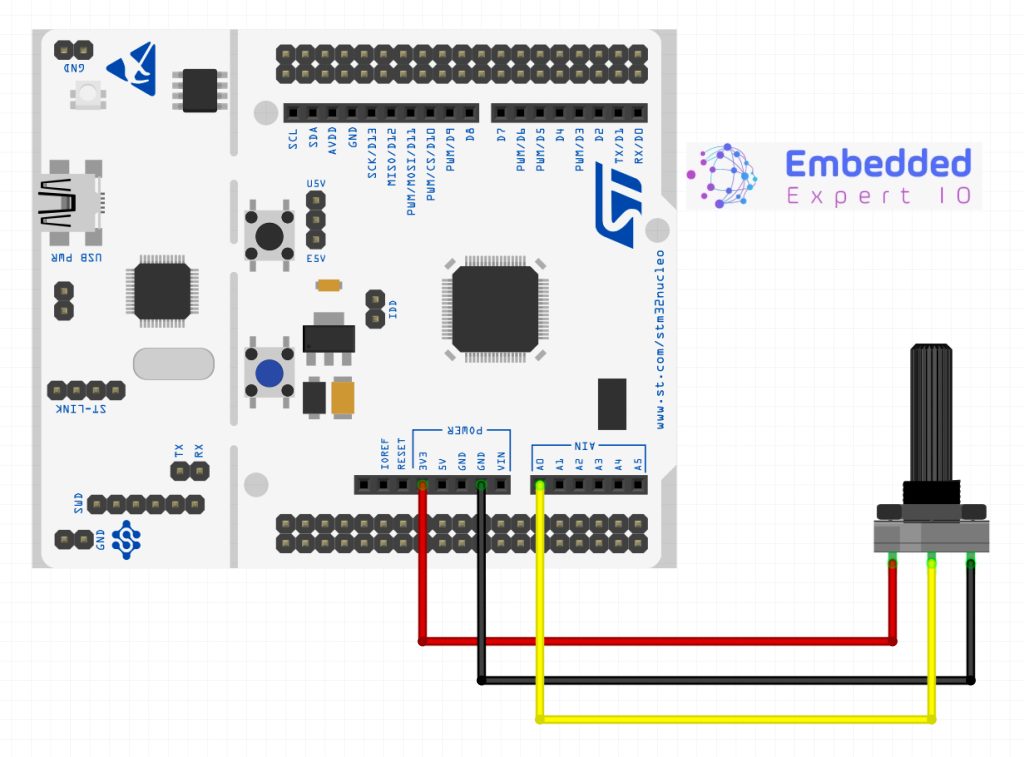
4. Connection:
The connection as following:
5. Results:
Start a debug session and add adcValue to live expression
When the pot is near the GND wire, you will get zero or near zero value as following:

On the other size of the pot:

We have successfully created first ADC drive.
However, this will block the CPU from doing anything during the conversion and getting the results.
This can be solved when interrupt shall be used.
Stay tuned.
Happy coding 😉
Add Comment