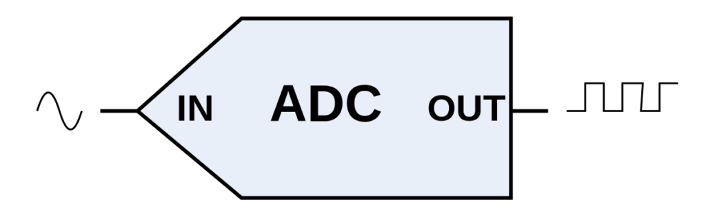
In the previous ADC guides (part 1, part 2, and part 3), we talked about how to configure the ADC to read a single channel in three different modes, polling, continuous with polling and interrupt. Those can be valid for simple application like temperature control of a room or heat-sink. However, in case multiple channel, ADC in interrupt is not recommended and requires careful management to acquire the data in correct sequence. This is when DMA come to solve the issue. In this guide, we shall look at the DMA and how to configure it to acquire the data from two channel.
In this guide we will cover the following:
- What is DMA
- Why should we use DMA when dealing with multiple channel in ADC
- Configuring the ADC and DMA
- Required parts, schematics and connection
- Code
- Result
1. What is DMA
DMA which stands for Direct Memory Access is part of MCU that handle data transfer from peripheral to memory without invoking CPU at all which relief cpu to do something else, like processing the acquired adc vlaue for dsp processing etc
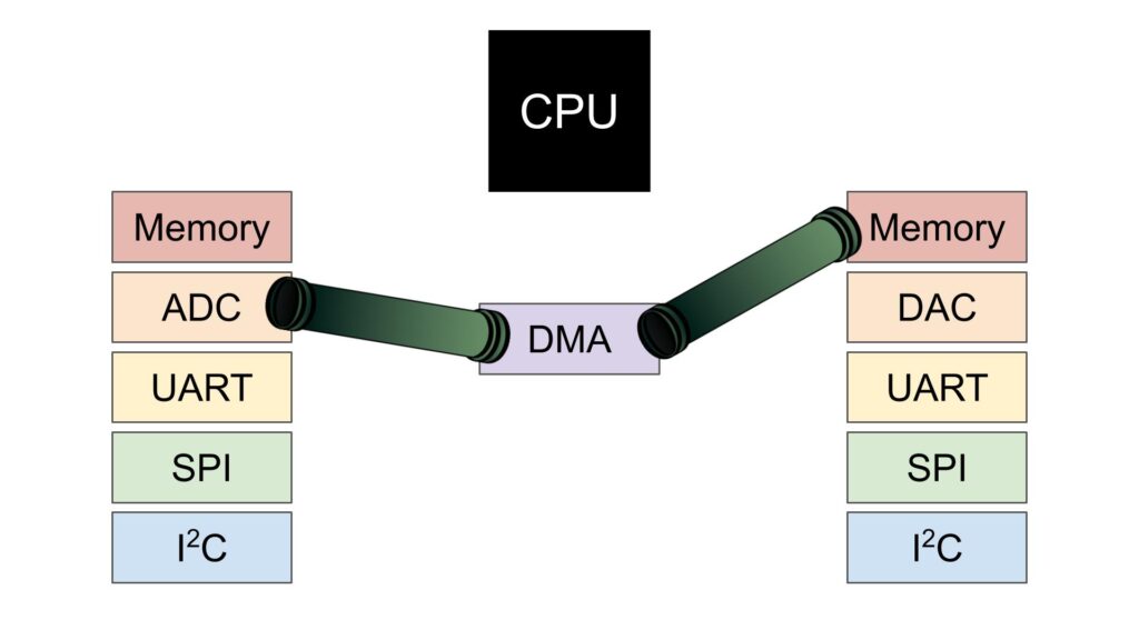
DMA can be operate in three different mode, Memory to Memory (moving one variable from one location to another), memory to peripheral (send string from memory to PC through UART) and peripheral to memory like in our case acquiring data from adc.
2. Why should we use DMA when dealing with multiple channel in ADC
Let say you want ti acquire data from adc from 3-channel in continuous mode. Since each conversion requires 15 cycles for 12-bit since the adc clock is the core frequency over (16MHz/2=8MHz), thats means generating interrupts at rate near half mega hertz which will effect the performance of the mcu. Hence, using DMA in such case makes sense.
3.1 Configure the ADC
To configure the ADC, first we enable GPIO clock access to the required pins (PA0 and PA1) in our case
RCC->AHB1ENR|=RCC_AHB1ENR_GPIOAEN;
then enabling adc clock
RCC->APB2ENR|=RCC_APB2ENR_ADC1EN;
After than we will configure PA0 and PA1 as analog inputs and PA5 as output
GPIOA->MODER|=GPIO_MODER_MODE0_0|GPIO_MODER_MODE0_1|GPIO_MODER_MODE1_0|GPIO_MODER_MODE1_1|GPIO_MODER_MODE5_0;
Setting the length of conversion to be 2 conversion as following
ADC1->SQR1|=(1<<20);
Set the sequence to be PA0 to be first and PA1 to seconds (from part 1)
ADC1->SQR3=(0U<<0)|(1U<<5);
Then enable continuous conversion, dma, scan mode and let the dma to be the controller
ADC1->CR1=ADC_CR1_SCAN;

ADC1->CR2|=ADC_CR2_DMA|ADC_CR2_DDS|ADC_CR2_CONT;
For now, we keep ADC disabled and enable it later
3.2 Configuring the DMA
We start by enabling DMA clock access
RCC->AHB1ENR |=RCC_AHB1ENR_DMA2EN;
Then disable the channel and wait until disabled
DMA2_Stream0->CR    &=~DMA_SxCR_EN;

while(DMA2_Stream0->CR ==DMA_SxCR_EN){;}
The we configure the DMA as following
Setting the dma to circular mode, memory and peripheral size of 16 bit and memory increment
DMA2_Stream0->CR |=DMA_SxCR_CIRC|DMA_SxCR_MSIZE_0|DMA_SxCR_PSIZE_0|DMA_SxCR_MINC;
Then selecting peripheral source to be the ADC1->DR
DMA2_Stream0->PAR =(uint32_t)(&(ADC1->DR));
then selecting memory location
DMA2_Stream0->M0AR =(uint32_t )(&adc_data);
Selecting how may transfer to be transferred (2 in this case)
DMA2_Stream0->NDTR =sizeof(adc_data)/sizeof(adc_data[0]);
Enable the stream
DMA2_Stream0->CR |=DMA_SxCR_EN;
Finally enable ADC and started as following
ADC1->CR2|=1;
ADC1->CR2|=ADC_CR2_SWSTART;
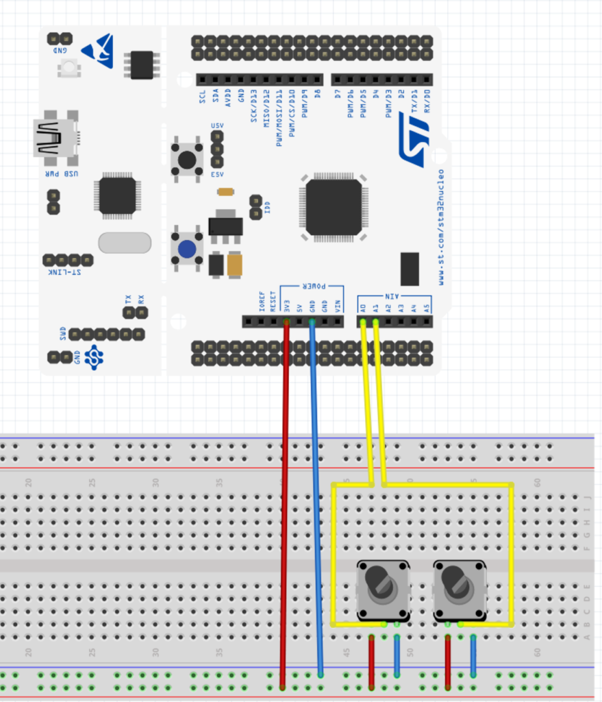
4.1 Required parts
In this guide we will need the following:
- STM32F411RE Nucleo
- 2x 1KOhm potentiometers
- Breadboard
- Hookup wires
4.2 Connection
5 Code and results
#include "stm32f4xx.h"                  // Device header
uint16_t adc_data[2]; 	                // array to hold adc_data
void delayMs(int delay) //inefficient delay for led blinking

{

int i;

for(; delay>0 ;delay--)

{

for(i =0; i<3195;i++);

}

}


int main(void)
	{
	RCC->AHB1ENR|=RCC_AHB1ENR_GPIOAEN;

	RCC->APB2ENR|=RCC_APB2ENR_ADC1EN;

	GPIOA->MODER|=GPIO_MODER_MODE0_0|GPIO_MODER_MODE0_1|GPIO_MODER_MODE1_0|GPIO_MODER_MODE1_1|GPIO_MODER_MODE5_0;

	ADC1->SQR1|=(1<<20);

	ADC1->SQR3=(0U<<0)|(1U<<5);

	ADC1->CR1=ADC_CR1_SCAN;

	ADC1->CR2|=ADC_CR2_DMA|ADC_CR2_DDS|ADC_CR2_CONT;

	RCC->AHB1ENR				|=RCC_AHB1ENR_DMA2EN;

	DMA2_Stream0->CR    &=~DMA_SxCR_EN;

	while(DMA2_Stream0->CR ==DMA_SxCR_EN){;}

	DMA2_Stream0->CR		|=DMA_SxCR_CIRC|DMA_SxCR_MSIZE_0|DMA_SxCR_PSIZE_0|DMA_SxCR_MINC;

	DMA2_Stream0->PAR		 =(uint32_t)(&(ADC1->DR));

	DMA2_Stream0->M0AR 	 =(uint32_t )(&adc_data);

	DMA2_Stream0->NDTR	 =sizeof(adc_data);


	DMA2_Stream0->CR		|=DMA_SxCR_EN;

	ADC1->CR2|=1;

	DMA2_Stream0->CR |= (1<<0);  // EN =1

	ADC1->CR2|=ADC_CR2_SWSTART;


	while(1)
		{
      //blinking led to demonisterate the dma capability
		GPIOA->ODR^=GPIO_ODR_OD5;
		delayMs(1000);
		}

	}
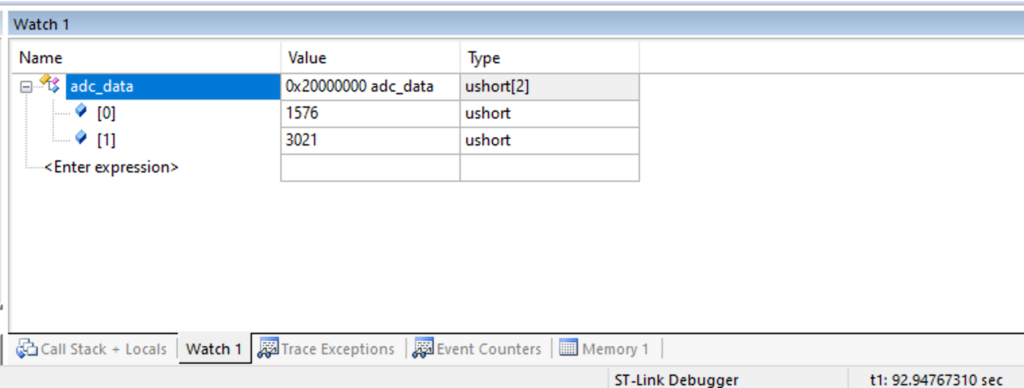
After you applied the code, rotate the pot and notice how they are changed without needing to update the value in the code.
This is how dma works in background without effecting the cpu performance.
3 Comments
well done, superior tut
I learn a lot from these article, when I try to use ADC+DMA without continuous, and no dma circular mode, I found dma transfer adc data correctly, next time, adc works, but dma not work, no data is transfered to memory, I try several days but all faild. I hope you colud give some tour for such problem, thanks.
You need to enable the DMA again once the DMA has finished transfer the data and an interrupt is generated.
Add Comment