In this guide, we shall use the DMA to update the duty cycle of the PWM to generate custom waveform like sinewave etc and the benefits of such approach.
In this guide, we shall cover the following:
- Why update PWM duty cycle using DMA.
- STM32CubeMX setup.
- Firmware development.
- Results.
1. Why Update PWM Duty Cycle using DMA:
Using DMA (Direct Memory Access) to update PWM (Pulse Width Modulation) in STM32H5 allows efficient transfer of data to a timer’s capture/compare registers without CPU intervention. This approach is particularly useful for applications requiring frequent or precise updates, such as motor control, waveform generation, or advanced lighting systems.
Here’s the theoretical explanation:
1. PWM Overview
PWM is generated using the timers in STM32, where the duty cycle and frequency are controlled by the values set in the timer’s ARR (Auto-Reload Register) and CCR (Capture/Compare Register). The CCR value determines the duty cycle, and changing it modifies the output waveform.
2. DMA Overview
DMA allows peripherals like timers to access memory directly, bypassing the CPU. This reduces CPU load and ensures data transfer happens quickly and deterministically.
3. Updating PWM Using DMA
The basic idea is to configure the DMA to transfer a buffer of duty cycle values to the timer’s CCR register, synchronized with the timer’s update event.
Key Steps
- Timer Configuration:
- Configure the timer for PWM output.
- Enable the DMA request for the timer update event. This ensures the DMA is triggered periodically.
- DMA Configuration:
- Set the memory source (e.g., an array of duty cycle values).
- Set the peripheral destination (the CCR register of the timer).
- Configure the DMA transfer mode:
- Circular Mode: Repeatedly cycle through the duty cycle array.
- Normal Mode: Transfer data once, then stop.
- Set the data size (16-bit or 32-bit, depending on the timer’s register size).
- Enable transfer complete interrupts if needed for additional logic.
- Trigger Synchronization:
- The DMA is triggered by the timer’s update event, ensuring the CCR is updated in sync with the PWM period.
4. Benefits of Using DMA for PWM Updates
- CPU Offloading: The CPU doesn’t need to manually update the CCR register.
- Precision: Updates occur at consistent intervals, avoiding jitter.
- Scalability: Multiple channels or arrays can be updated simultaneously using different DMA streams.
- Power Efficiency: Reduces CPU activity, saving power in embedded systems.
5. Use Case Example
If you’re generating a waveform:
- Create an array with pre-calculated duty cycle values representing the waveform (e.g., sine wave).
- Use DMA to transfer these values to the timer’s CCR register.
- The timer’s update event triggers the DMA transfer, ensuring the PWM signal represents the desired waveform.
6. Timer and DMA Interaction
- DMA Request: The timer generates a DMA request signal on every update event (or other configured events like capture/compare match).
- DMA Transfer: On receiving the request, the DMA transfers the next value from memory to the timer’s CCRregister.
- PWM Output: The timer updates the PWM output at the next cycle based on the new CCR value.
7. Practical Considerations
- Buffer Size: Ensure the buffer contains enough data for your application.
- DMA Priority: Set appropriate priority to avoid conflicts with other peripherals.
- Synchronization: Ensure the timer’s period matches the data update rate for smooth operation.
- Cache Management: For STM32H5, ensure proper handling of cached data when using DMA. Mark the buffer as non-cacheable or use cache maintenance functions to ensure DMA accesses the correct data.
2. STM32CubeMX Setup:
We start off by creating new project with name of PWM_DMA. For how to create project using STM32CubeIDE, please refer to this guide here.
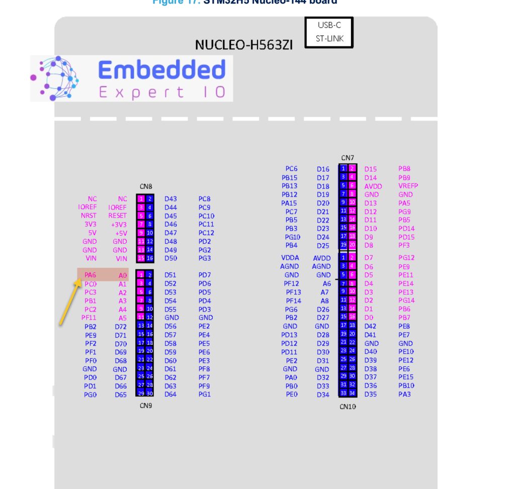
Since STM32H563Zi Nucleo-144 has arduino pinout, we can use that.
From the user guide of STM32H563ZI Nucleo-144 we can find that A0 of Arduino pin is connected to PA6 as following:
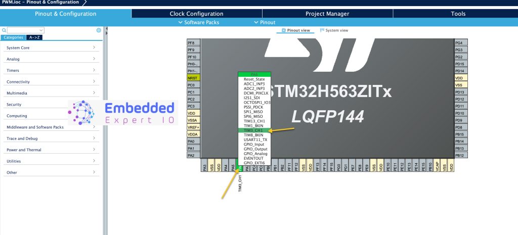
From STM32CubeIDE enable PA6 as TIM3_CH1 as following:
Next, from timers section, enable TIM3 as following:
- Set the clock source to be internal.
- Enable Channel 1 to be in PWM mode as following:
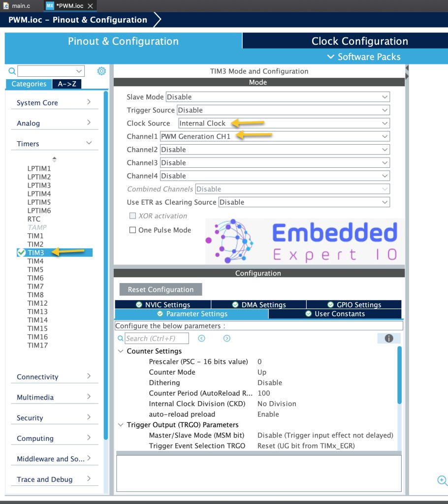
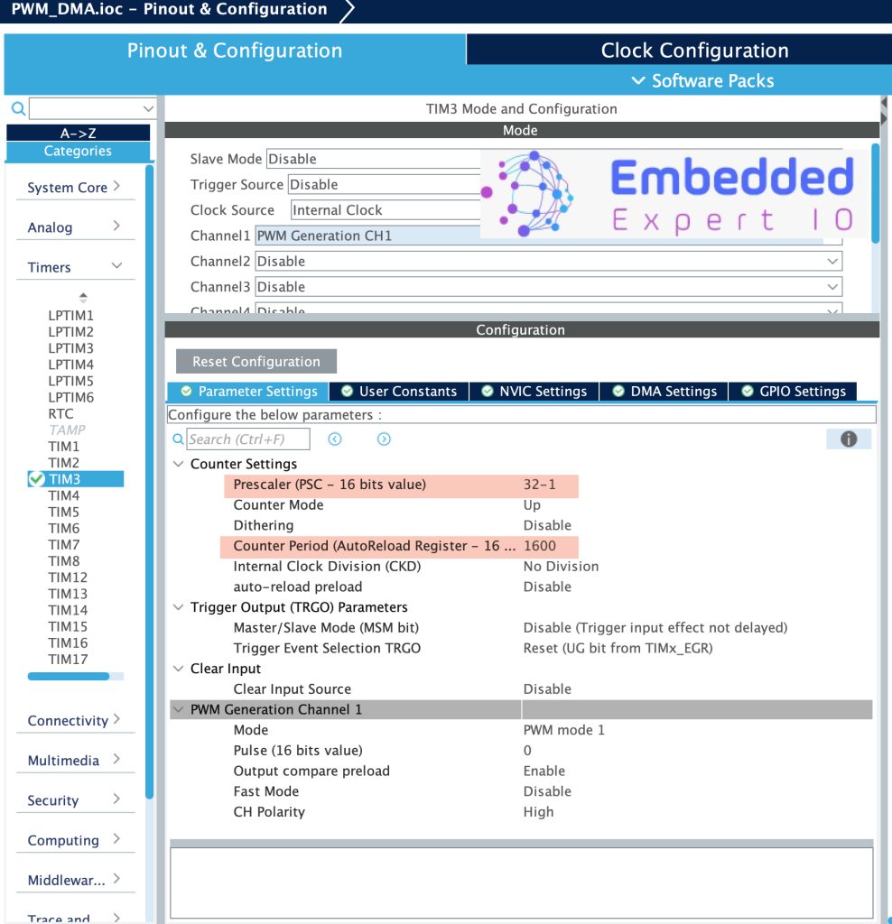
Next, set the parameters of the timer as following:
- Set the prescaler to 32-1 This will give us 1MHz (According to your application).
- Set the ARR to 1600, this will reduce the frequency of the PWM to 625Hz (According to your application).
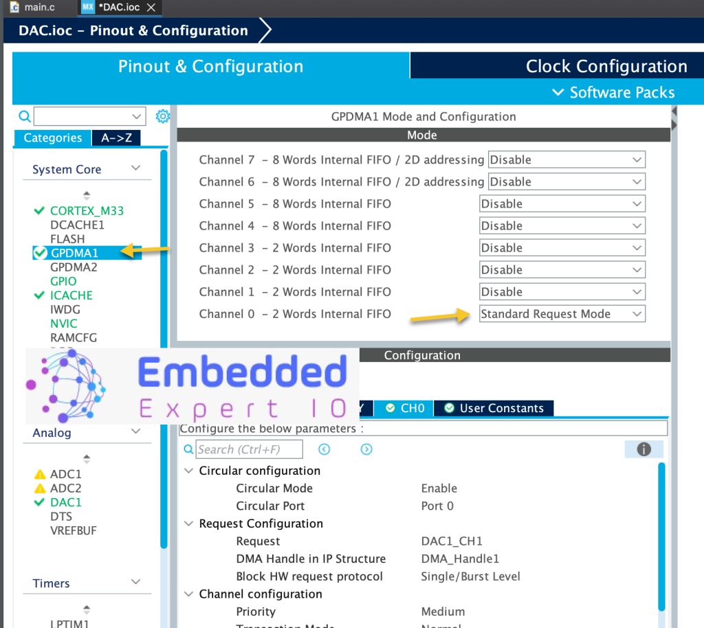
Next, in GPDMA1, enable Ch0 in standard request mode as following:
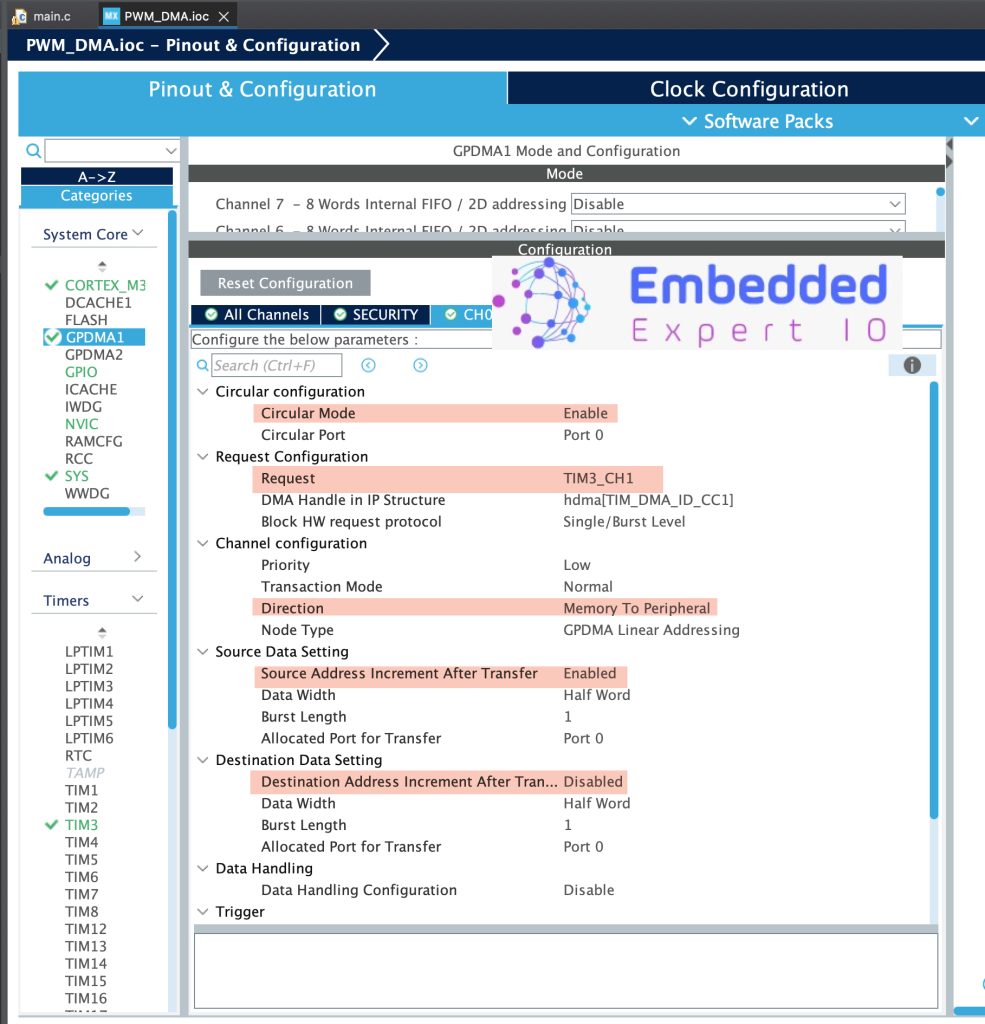
Next configure the DMA as following:
- Circular Mode to Enable.
- Request is TIM3_CH1.
- Set the direction to be Memory to Peripheral.
- From Data source, set the address increment to enabled and data width to half-word.
- From Destination data, set the data width to half word and make sure address increment is disabled.
Thats all for the STM32CubeMX configuration.
Save the project and this shall generate the project.
3. Firmware Development:
Once the project has been generated, main.c shall be opened.
In main.c, in user begin PV (private variables), declare the following array:
#define sample_size		220


uint16_t lookUp1[sample_size] = {0,50 ,100 ,151 ,201 ,250 ,300 ,349 ,398 ,446 ,494 ,542 ,589 ,635 ,681
	,726 ,771 ,814 ,857 ,899 ,940 ,981 ,1020 ,1058 ,1095 ,1131 ,1166 ,1200 ,1233 ,1264
	,1294 ,1323 ,1351 ,1377 ,1402 ,1426 ,1448 ,1468 ,1488 ,1505 ,1522 ,1536 ,1550 ,1561
	,1572 ,1580 ,1587 ,1593 ,1597 ,1599 ,1600 ,1599 ,1597 ,1593 ,1587 ,1580 ,1572 ,1561
	,1550 ,1536 ,1522 ,1505 ,1488 ,1468 ,1448 ,1426 ,1402 ,1377 ,1351 ,1323 ,1294 ,1264
	,1233 ,1200 ,1166 ,1131 ,1095 ,1058 ,1020 ,981 ,940 ,899 ,857 ,814 ,771 ,726 ,681 ,635
	,589 ,542 ,494 ,446 ,398 ,349 ,300 ,250 ,201 ,151 ,100 ,50,0 ,0 ,0 ,0 ,0 ,0 ,0 ,0 ,0 ,0
	,0 ,0 ,0 ,0 ,0 ,0 ,0 ,0 ,0 ,0 ,0 ,0 ,0 ,0 ,0 ,0 ,0 ,0 ,0 ,0 ,0 ,0 ,0 ,0 ,0 ,0 ,0 ,0 ,0 ,0
	,0 ,0 ,0 ,0 ,0 ,0 ,0 ,0 ,0 ,0 ,0 ,0 ,0 ,0 ,0 ,0 ,0 ,0 ,0 ,0 ,0 ,0 ,0 ,0 ,0 ,0 ,0 ,0 ,0 ,0
	,0 ,0 ,0 ,0 ,0 ,0 ,0 ,0 ,0 ,0 ,0 ,0 ,0 ,0 ,0 ,0 ,0 ,0 ,0 ,0 ,0 ,0 ,0 ,0 ,0 ,0 ,0 ,0 ,0 ,0 };
This is an example array, it will depend on your application.
In user code begin 2 of the main function, we shall start the timer in PWM mode with DMA as following:
HAL_TIM_PWM_Start_DMA(&htim3, TIM_CHANNEL_1, (uint32_t)&lookUp1, sizeof(lookUp1));
The function, HAL_TIM_PWM_Start_DMA takes the following parameters:
- Handletypedef for the timer which is timer 3 (htim3) in this case.
- Timer channel which is channel 1 (TIM_CHANNEL_1).
- Array which hold the duty cycle array.
- Size of the array.
hats all for the firmware development.
Save the project, build it and run it on your STM32H563Zi board.

4. Results:
By probing PA6 with either oscilloscope or logic analyzer, you should get the following:

Note: If you are using logic analyzer, it will appear slightly different.
Happy coding 😉
Add Comment