
In the previous guide (here), we took a look at the PWM mode in timer2 of STM32L053. In this guide, we shall take a look at the output compare where the the output will be toggled each time the timer overflow.
In this guide we cover the following:
- What is output compare mode.
- Configure the timer and GPIO for output compare mode.
- Code.
- Demo.
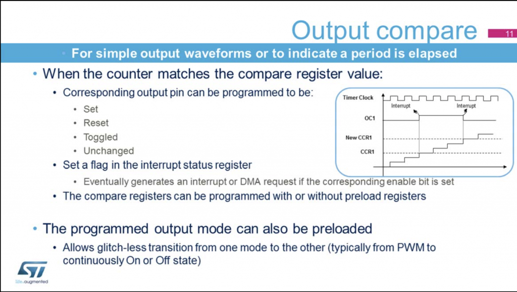
1. What is Output Compare Mode:
In this mode, the timer shall count to the maximum level (set by the ARR), the following will happen:
- Assigns the corresponding output pin to a programmable value defined by the output compare mode.
- Sets a flag in the interrupt status register.
- Generates an interrupt if the corresponding interrupt mask is set.
- Sends a DMA request if the corresponding enable bit is set.
In our case, we will toggle PA0(TIM2_CH1) and PA1 (TIM2_CH2) based on out setting.
2. Configure the timer and GPIO for output compare mode:
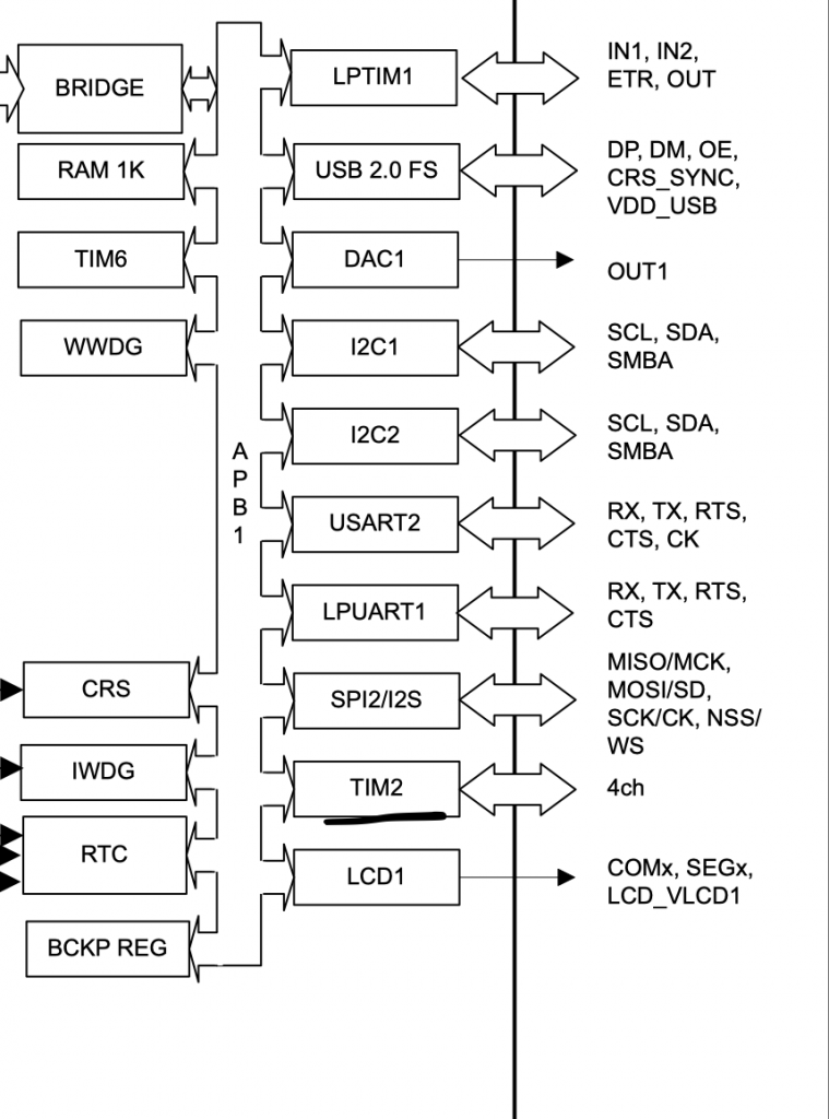
First we need to locate which pins connected to TIMER2_CH1 and TIMER2_CH2.
From the datasheet, we can find the related timer channels:
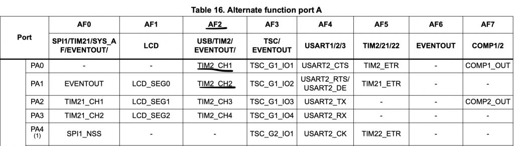
From the datasheet, the pins are related to timer1 are PA0 and PA1 and also the alternative function is AF2 and we can create a symbolic name as following:
#define TIM2_AF 0x02
Then we can enabled clock access to GPIOA as following:
In order to enable clock access to the GPIOA, we need to go to reference manual and check the register named GPIO clock enable register.
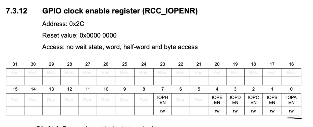
Hence, we need to set bit0 to 1 and we can use CMSIS macros to do it as following:
	/*Enable clock access to GPIOA*/
	RCC->IOPENR |= RCC_IOPENR_GPIOAEN;
Then we shall set the mode of the pin to be alternate fuction:
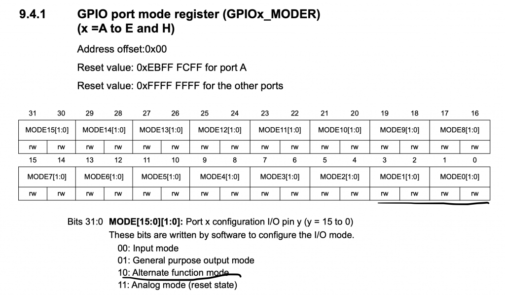
	/*Set PA0 and PA1 to alternate function*/
	GPIOA->MODER|=GPIO_MODER_MODE0_1|GPIO_MODER_MODE1_1;
	GPIOA->MODER&=~(GPIO_MODER_MODE0_0|GPIO_MODER_MODE1_0);
Then set which alternate function shall be used from GPIO alternate function low register (AFR[0]):
	/*Select which alternate function*/
	GPIOA->AFR[0]|=(TIM2_AF<<0)|(TIM2_AF<<4);
Now we can configure the timer to generate PWM signal
We start off by enabling clock access to TIMER2 as following:
RCC->APB1ENR|=RCC_APB1ENR_TIM2EN;
Set the prescaler and ARR to 2097 & 100 respectively:
	TIM2->PSC=2097;
	TIM2->ARR=100;
In order to configure the timer to work in PWM, this where TIM capture/compare mode register 1 will come to play, this register responsible to CH1 and CH2.
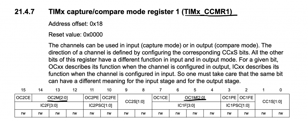
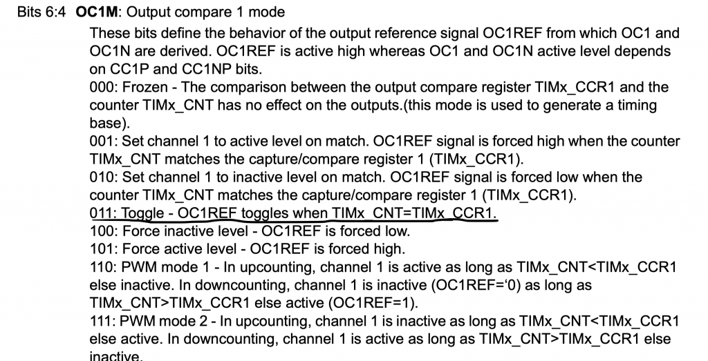
Hence, bit 4 and 5 for CH1 to be in toggle, bit 12 and 13 for CH2 to be in toggle.
TIM2->CCMR1|=TIM_CCMR1_OC1M_0|TIM_CCMR1_OC1M_1|TIM_CCMR1_OC2M_0|TIM_CCMR1_OC2M_1;
Then, capture compare shall be enabled and invert the CH1:
TIM2->CCER|=TIM_CCER_CC1E|TIM_CCER_CC2E|TIM_CCER_CC2P;
Set both CCR1 and CCR2 to zero:
	TIM2->CCR1=0;
	TIM2->CCR2=0;
Finally, enable the timer:
TIM2->CR1|=TIM_CR1_CEN;
3. Code:
Hence the entire code as following:
/*Enable clock access to GPIOA*/
	RCC->IOPENR |= RCC_IOPENR_GPIOAEN;
	/*Set PA0 and PA1 to alternate function*/
	GPIOA->MODER|=GPIO_MODER_MODE0_1|GPIO_MODER_MODE1_1;
	GPIOA->MODER&=~(GPIO_MODER_MODE0_0|GPIO_MODER_MODE1_0);


	/*Select which alternate function*/
	GPIOA->AFR[0]|=(TIM2_AF<<0)|(TIM2_AF<<4);

	/**Configure timer 2 in PWM mode */

	RCC->APB1ENR|=RCC_APB1ENR_TIM2EN;
	TIM2->PSC=2097;
	TIM2->ARR=1000;
	TIM2->CCMR1|=TIM_CCMR1_OC1M_0|TIM_CCMR1_OC1M_1|TIM_CCMR1_OC2M_0|TIM_CCMR1_OC2M_1;
	TIM2->CCER|=TIM_CCER_CC1E|TIM_CCER_CC2E|TIM_CCER_CC2P;
	TIM2->CCR1=0;
	TIM2->CCR2=0;
	TIM2->CR1|=TIM_CR1_CEN;
4. Demo:
Happy coding 🙂
Add Comment