The Serial Peripheral Interface (SPI) is a bus interface found in many devices such as DAC,ADC, EEPROM etc. SPI devices typically use two pin for data transfer. – SDI and SDO. The SPI bus has the SCLK (Serial Clock) pin to synchronize the data transfer between two chips. It has has the CE (Chip Enable )pin to initiate and terminate the data transfer. These four pins-SDI,SDO,SCLK and CE form the 4-wire interface of SPI. In many modules, these pins are often referred to ad the MOSI,MISO,SCK and SS pins
Clock Polarity
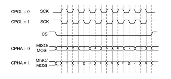
In SPI communication, both master and slave uses the same clock but the master and slave( s) must agree on the clock polarity and phase with respect to the data. Freescale names these two options as CPOL (clock polarity) and CPHA (clock phase) respectively, and most companies have adopted that convention. At CPOL = 0 the idle value of the clock is zero while at CPOL = 1 the idle value of the clock is one. CPHA = 0 means sample data on the leading (first) clock edge, while CPHA = 1 means sample data on the trailing (second) clock edge. Notice that if the idle value of the clock is zero the leading (first) clock edge is a rising edge but if the idle value of the clock is one, the leading (first) clock edge is a falling edge. See the figure below.
Programming the SPI
To program the SPI, follow the steps below (We are using the tm4c123 tiva C launchpad for this example)
1. Enable the clock to GPIO pin by using RCGCGPIO. 2. Set the GPIO AFSEL (GPIO alternate function) for SSI pins. 3. Enable digital pins in the GPIODEN (GPIO Digital enable) register. 4. Assign the SPI signals to specific pins using GPIOCTL register.
After the GPIO configuration, we need to take the following steps to configure the SSI for the SPI protocol: 1. Enable the clock to SSI module using RCGCSSI.
2. Disable the SSI via bit 1 of SSICR1 register before initialization.
3. Set the Bit Rate with the SSICPSR prescaler and SSICR0 control registers.
4. Also select the SPI mode, phase, polarity, and data size in SSICR0 control register.
5. Select the master mod in SSISCR1 register.
6. Enable SSI using SSICR1 register.
7. Assert slave select signal.
8. Wait until the TNF flag (transmit FIFO not full) in SSISR (status register) goes high, then load a byte of data into SSIDR (data register) to be transmitted.
9. Repeat step 8 above until all the data are in the FIFO.
10. Wait until transmit is complete (transmit FIFO empty and SSI not busy). 11. De-assert the slave select signal.
/* PORTD 0 - SSI1 clock
 PORTD 3 - SSI1 Tx
 PORTF 2 - slave select
 Generate sawtooth on output A */

#include "TM4C123GH6PM.h"

void init_SSI1(void);
void LTC1661Write(int chan, short d);

int main(void)
{
    int i;

    init_SSI1();

    for(;;)
    {
        for (i = 0; i < 1023; i++)
        {
            LTC1661Write(0, i); /* write a sawtooth to channel A */
        }
    }
}

void LTC1661Write(int chan, short data)
{
    GPIOF->DATA &= ~0x04;       /* assert SS low */
    data = (data & 0x03FF) << 2; /* bit 1-0 unused */
    if (chan == 0)              /* add control code with channel number */
        data |= 0x9000;
    else
        data |= 0xA000;
    while((SSI1->SR & 2) == 0); /* wait until FIFO not full */
    SSI1->DR = data >> 8;       /* transmit high byte */
    while((SSI1->SR & 2) == 0); /* wait until FIFO not full */
    SSI1->DR = data & 0xFF;     /* transmit low byte */
    while(SSI1->SR & 0x10);     /* wait until transmit complete */
    GPIOF->DATA |= 0x04;        /* keep SS idle high */
}

void init_SSI1(void)
{
    SYSCTL->RCGCSSI |= 2;       /* enable clock to SSI1 */
    SYSCTL->RCGCGPIO |= 8;      /* enable clock to GPIOD for SSI1 */
    SYSCTL->RCGCGPIO |= 0x20;   /* enable clock to GPIOF for slave select */

    /* configure PORTD 3, 1 for SSI1 clock and Tx */
    GPIOD->AMSEL &= ~0x09;      /* disable analog for these pins */
    GPIOD->DEN |= 0x09;         /* and make them digital */
    GPIOD->AFSEL |= 0x09;       /* enable alternate function */
    GPIOD->PCTL &= ~0x0000F00F; /* assign pins to SSI1 */
    GPIOD->PCTL |= 0x00002002;  /* assign pins to SSI1 */

    /* configure PORTF 2 for slave select */
    GPIOF->DEN |= 0x04;         /* make the pin digital */
    GPIOF->DIR |= 0x04;         /* make the pin output */
    GPIOF->DATA |= 0x04;        /* keep SS idle high */

    /* SPI Master, POL = 0, PHA = 0, clock = 4 MHz, 16 bit data */
    SSI1->CR1 = 0;          /* disable SSI and make it master */
    SSI1->CC = 0;           /* use system clock */
    SSI1->CPSR = 2;         /* prescaler divided by 2 */
    SSI1->CR0 = 0x0007;     /* 8 MHz SSI clock, SPI mode, 8 bit data */
    SSI1->CR1 |= 2;         /* enable SSI1 */
}
Add Comment