In this guide, we shall take a look at MAX7219 8-Digit LED Display Drivers and how to use them with STM32.
In this guide, we shall cover the following:
- MAX7219
- Connection with STM32
- Code
- Demo
1.1 MAX7219:
Unlike the 74HC595 shift register, we don’t need to control each digit of 7-segment display individually by adding delay. We just send data 7-segments and seven-segment control data. It has a built-in BCD to 7-segment decoder. Most importantly, it has on-chip 8×8 RAM which we can use to store display codes of digits that we want to display.
One of the major advantages of this display driver is that we can update individual bits without updating the entire display that isn’t possible with 74HC595 shift register. Hence, we can save microcontroller execution time and energy.
Moreover, it has a built-in brightness control circuit and by using a scan limit register we can configure the number of digits display we want to use.
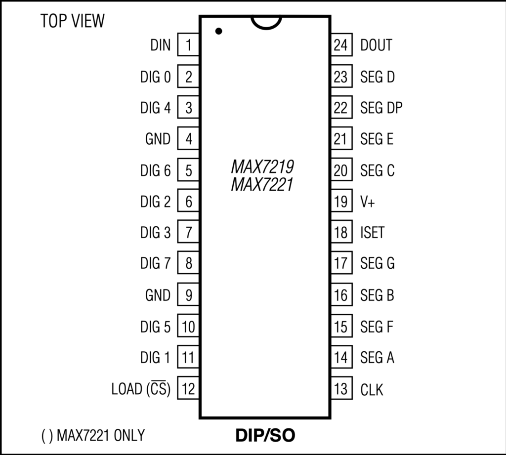
1.2 Pinout Diagram:
As you can depict from this pinout diagram that it is a 24 pin IC. Eight pins provide data to segments that A-G pins. DIG0 to DIG7 pins are used to connect with common pins of 8 common-cathode type seven-segment displays. The pin configuration is the same for both MAX7219 and MAX7212.
This table shows the function of each pin. Out of 14 pins, 16 pins are used to connect 8-digit LED displays.
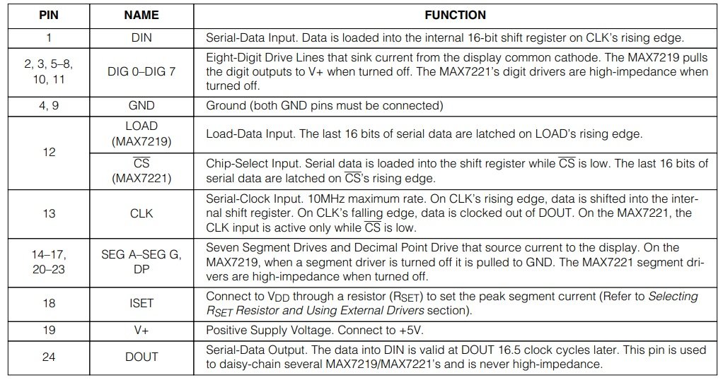
According to the above table, MAX7219/MAX7212 receives and transmits data through SPI communication. Pin1 (DIN) is a serial data input pin. We connect DIN of MAX7219 with a DOUT pin of PIC16F877A microcontroller SPI pin. Serial data transfer to an internal 16-bit register on every positive edge clock on pin13(Clk). We provide clock signals from Pic microcontroller SPI communication clock pin (SCK).
1.3 MAX7219/MAX7212 Registers:
This block diagram shows the configuration registers of MAX7219 LED driver IC. It has drivers for segements and digits.
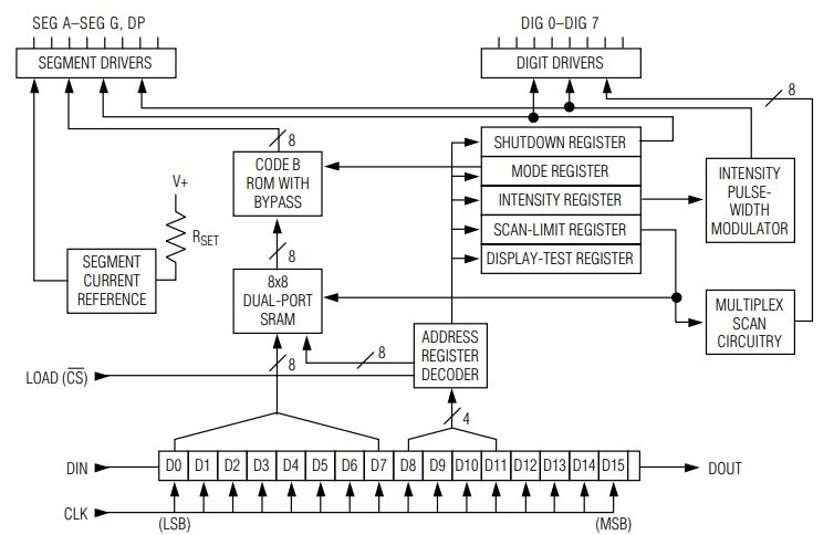
Following are the main registers that used to configure and control display.
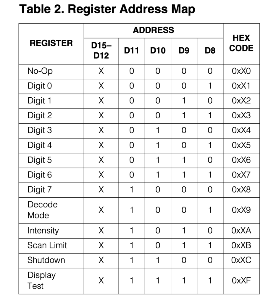
1.4 Registers Map:
The following table shows the registers within the IC.
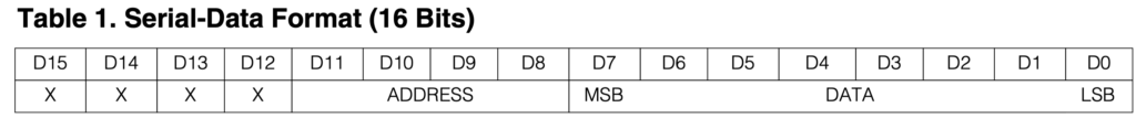
1.5 Serial Data Format:
The data shall be sent in serial format with most significant bit (MSB) first to be transmit:
2. Connection with STM32:
The connection as following:
| MAX7219 | STM32F411 Nucleo |
| Vcc | 5V |
| GND | GND |
| Din | MOSI (PA7) |
| SCK | SCK (PA7) |
| CS | PA9 |
3. Code
We start off by configuring the SPI as following:
void spi_gpio_init(void)
{
	/*Enable clock access to GPIOA*/
	RCC->AHB1ENR |= GPIOAEN;

	/*Set PA5,PA6,PA7 mode to alternate function*/

	/*PA5*/
	GPIOA->MODER &=~(1U<<10);
	GPIOA->MODER |=(1U<<11);

	/*PA6*/
	GPIOA->MODER &=~(1U<<12);
	GPIOA->MODER |=(1U<<13);

	/*PA7*/
	GPIOA->MODER &=~(1U<<14);
	GPIOA->MODER |=(1U<<15);


	/*Set PA9 as output pin*/
	GPIOA->MODER |=(1U<<18);
	GPIOA->MODER &=~(1U<<19);

	/*Set PA5,PA6,PA7 alternate function type to SPI1*/
	/*PA5*/
	GPIOA->AFR[0] |=(1U<<20);
	GPIOA->AFR[0] &= ~(1U<<21);
	GPIOA->AFR[0] |=(1U<<22);
	GPIOA->AFR[0] &= ~(1U<<23);

	/*PA6*/
	GPIOA->AFR[0] |=(1U<<24);
	GPIOA->AFR[0] &= ~(1U<<25);
	GPIOA->AFR[0] |=(1U<<26);
	GPIOA->AFR[0] &= ~(1U<<27);

	/*PA7*/
	GPIOA->AFR[0] |=(1U<<28);
	GPIOA->AFR[0] &= ~(1U<<29);
	GPIOA->AFR[0] |=(1U<<30);
	GPIOA->AFR[0] &= ~(1U<<31);


}

void spi1_config(void)
{
	/*Enable clock access to SPI1 module*/

	RCC->APB2ENR|=RCC_APB2ENR_SPI1EN; //enable clock for spi1

	SPI1->CR2=0;
	SPI1->CR1=SPI_CR1_SSM|SPI_CR1_MSTR|SPI_CR1_SSI|SPI_CR1_SPE;
}
SPI write function for multiple bytes as following:
void spi1_transmit(uint8_t *data,uint32_t size)
{

	uint32_t i=0;
	uint8_t temp;

	while(i<size)
	{
		/*Wait until TXE is set*/
		while(!(SPI1->SR & (SR_TXE))){}

		/*Write the data to the data register*/
		SPI1->DR = data[i];
		i++;
	}
	/*Wait until TXE is set*/
	while(!(SPI1->SR & (SR_TXE))){}

	/*Wait for BUSY flag to reset*/
	while((SPI1->SR & (SR_BSY))){}

	/*Clear OVR flag*/
	temp = SPI1->DR;
	temp = SPI1->SR;

}
Chip enable disable function :
void cs_enable(void)
{
	GPIOA->ODR &=~(1U<<9);

}

/*Pull high to disable*/
void cs_disable(void)
{
	GPIOA->ODR |=(1U<<9);
}
Now for MAX7219, we can need to initialize the IC first as following:
void max7219_init(void)
		{
		spi_gpio_init();
		spi1_config();
		uint8_t data[2];
		  // Run test
			// All LED segments should light up
		data[0]=0x0F;
		data[1]=0x01;
		cs_enable();
		spi1_transmit(data,2);
		cs_disable();
		for (volatile int i=0;i<100000;i++){}
		data[0]=0x0F;
		data[1]=0x00;
		cs_enable();
		spi1_transmit(data,2);
		cs_disable();
		// Enable mode B
		data[0]=0x09;
		data[1]=0xFF;
		cs_enable();
		spi1_transmit(data,2);
		cs_disable();
		 // Use lowest intensity
		data[0]=0x0A;
		data[1]=0x0F;
		cs_enable();
		spi1_transmit(data,2);
		cs_disable();
	 //  scan all digit
		data[0]=0x0B;
		data[1]=0x07;
		cs_enable();
		spi1_transmit(data,2);
		cs_disable();
		// Turn on chip
		data[0]=0x0C;
		data[1]=0x01;
		cs_enable();
		spi1_transmit(data,2);

		cs_disable();
		// clear display
		for (int i=0;i<9;i++)
					{
					display_number(i,0x0f);
					}

		}
For displaying single number on single digit, we can use the following:
void  display_number (uint8_t digit, uint8_t number)
			{

		uint8_t data[2];
		data[0]=digit; data[1]=number;
		cs_enable();
		spi1_transmit(data,2);
   	cs_disable();
  }
For clearing the display:
void clear_display(void)
		{

		for (int i=0;i<9;i++)
					{
					display_number(i,0x0f);
					}

		}
Now, in main file, we can call the initializing function and start display numbers as following:
#include "max7219.h"


int main(void)
	{
	for(volatile int i=0;i<100000;i++){}
		max7219_init();
	for(volatile int i=0;i<100000;i++){}
		while(1)
			{
			for (int i=0;i<9;i++)
				{
					for (int j=0;j<10;j++)
						{
							display_number(i,j);
							for (volatile int k=0;k<200000;k++){}
						}


				}
			for (volatile int k=0;k<200000;k++){}
			clear_display();

				}

	}
You can download the source code from here:
4. Demo:
Happy coding :
Add Comment