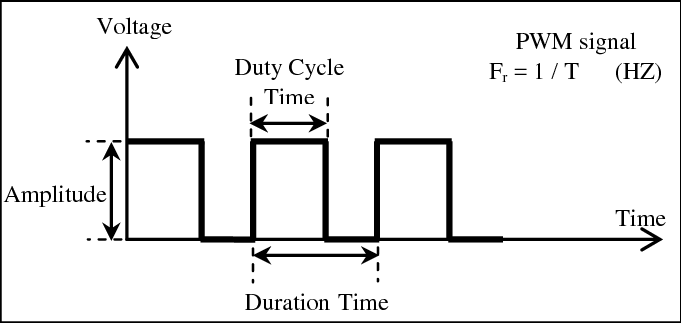
In the previous guide (here), we took a look at how to configure the timer in PWM and we were able to update the duty cycle of the PWM to fade two LEDs using polling mode. In this guide, we shall look how to configure timer to update the duty cycle using DMA (Direct Memory Access).
In this guide, we will cover the following:
- Configure the timer in PWM.
- Configure the DMA.
- Code.
- Demo
1. Configure the Timer in PWM Mode:
We start off by configuring the GPIO (check the topic here):
void GPIO_Init(void)
{
	#define AF01 0x01
	RCC->AHB1ENR|=RCC_AHB1ENR_GPIOAEN|RCC_AHB1ENR_GPIOBEN;
	GPIOA->MODER|=GPIO_MODER_MODE0_1|GPIO_MODER_MODE1_1;
	GPIOA->AFR[0]|=(0x01<<0)|(0x01<<4);

}
Then we enable clock access to timer2 and configure the prescaler and ARR value:
RCC->APB1ENR|=RCC_APB1ENR_TIM2EN; //enable clock access tto tim2
TIM2->PSC=0; //set prescaller to 0 (no divider)
TIM2->ARR=1600; //set the maximum count value
TIM2->CNT=0; //seset the current count
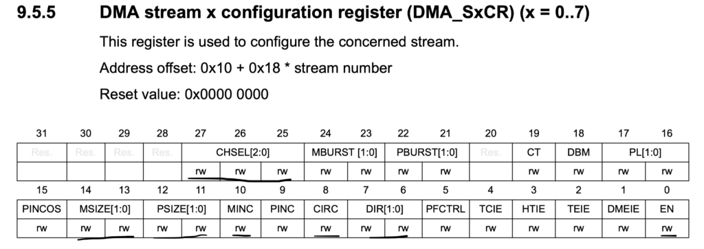
Now, in order to make the timer work with the DMA, we need to configure CCDS: Capture/compare DMA selection in Control Register 2 (CR2):
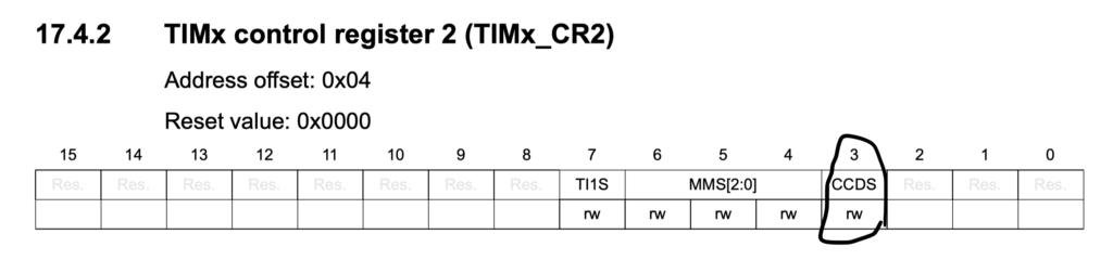
- CCDS: Capture/compare DMA selection
TIM2->CR2|=TIM_CR2_CCDS;
From DMA/Interrupt enable register, we need to enable the following:
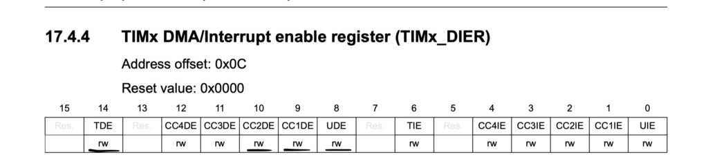
- UDE: Update DMA request enable
- CC1DE: Capture/Compare 1 DMA request enable
- CC2DE: Capture/Compare 2 DMA request enable
- TDE: Trigger DMA request enable
TIM2->DIER|=(TIM_DIER_UDE)|TIM_DIER_CC1DE|TIM_DIER_CC2DE;
TIM2->DIER|=TIM_DIER_TDE;
Finally enable the PWM channel:
TIM2->CCMR1=TIM_CCMR1_OC1M_2|TIM_CCMR1_OC1M_1|TIM_CCMR1_OC2M_2|TIM_CCMR1_OC2M_1; //configure the pins as PWM
TIM2->CCER|=TIM_CCER_CC1E|TIM_CCER_CC2E; //enbale channel1 and channel2
Please note that we didn’t start the timer yet.
2. Configuring the DMA:
Before configuring the DMA, we need to know which DMA, stream and channel to use.
From the reference manual, DMA section, we can find DMA request map
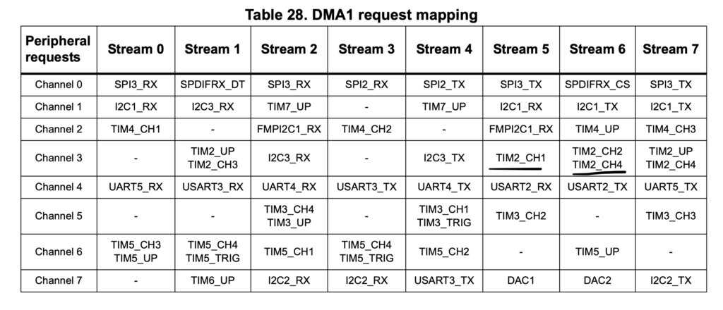
Hence, we need to use DMA1, Stream5 and Stream6 and channel 3
We can start by enabling clock access to DMA1 as following:
RCC->AHB1ENR|=RCC_AHB1ENR_DMA1EN;
The disable the stream and wait until it is disabled
RCC->AHB1ENR|=RCC_AHB1ENR_DMA1EN;
DMA1_Stream5->CR&=DMA_SxCR_EN;
while((DMA1_Stream5->CR)&DMA_SxCR_EN){;}

DMA1_Stream6->CR&=DMA_SxCR_EN;
while((DMA1_Stream6->CR)&DMA_SxCR_EN){;}
Then we can configure both stream as following:
- Channel 3
- Memory size to 32
- Peripheral size to 32
- Memory increment mode
- Circular mode
- Direction memory to peripheral
#define CH3   ((1<<26)|(1<<25))
#define M_SI32 (1<<14)
#define P_SI32 (1<<12)
#define M_INC  (1<<10)
#define Cir    (1<<8)
#define M2P    (1<<6)
DMA1_Stream5->CR|=CH3|M_SI32|P_SI32|M_INC|Cir|M2P;
DMA1_Stream6->CR|=CH3|M_SI32|P_SI32|M_INC|Cir|M2P;
Set number of transfer to 200 (in this case):
DMA1_Stream5->NDTR=(uint16_t)200;
DMA1_Stream6->NDTR=(uint16_t)200;
Peripheral address to be CCR1 for Stream5
DMA1_Stream5->PAR=(uint32_t)(&TIM2->CCR1);
CCR2 for Stream6
DMA1_Stream6->PAR=(uint32_t)(&TIM2->CCR2);
Memory address to be lookup table 1 for Stream5
DMA1_Stream5->M0AR=(uint32_t)(&lookUp1);
lookup table 2 for Stream6
DMA1_Stream6->M0AR=(uint32_t)(&lookUp2);
Enable both stream:
DMA1_Stream6->CR|=DMA_SxCR_EN;

DMA1_Stream5->CR|=DMA_SxCR_EN;
and Finally enable the timer:
TIM2->CR1|=1; //enable timer
3. Code:
Hence the entire code shall be like this:
#include "stm32f4xx.h"                  // Device header

#define CH3   ((1<<26)|(1<<25))
#define M_SI32 (1<<14)
#define P_SI32 (1<<12)
#define M_INC  (1<<10)
#define Cir    (1<<8)
#define M2P    (1<<6)
#define PFCTRL (1<<5)
// Look up tables with 200 entries each, normalised to have max value of 1600 which is the period of the PWM loaded into register ICR1.
uint32_t lookUp1[] = {0,50 ,100 ,151 ,201 ,250 ,300 ,349 ,398 ,446 ,494 ,542 ,589 ,635 ,681
	,726 ,771 ,814 ,857 ,899 ,940 ,981 ,1020 ,1058 ,1095 ,1131 ,1166 ,1200 ,1233 ,1264
	,1294 ,1323 ,1351 ,1377 ,1402 ,1426 ,1448 ,1468 ,1488 ,1505 ,1522 ,1536 ,1550 ,1561
	,1572 ,1580 ,1587 ,1593 ,1597 ,1599 ,1600 ,1599 ,1597 ,1593 ,1587 ,1580 ,1572 ,1561
	,1550 ,1536 ,1522 ,1505 ,1488 ,1468 ,1448 ,1426 ,1402 ,1377 ,1351 ,1323 ,1294 ,1264
	,1233 ,1200 ,1166 ,1131 ,1095 ,1058 ,1020 ,981 ,940 ,899 ,857 ,814 ,771 ,726 ,681 ,635
	,589 ,542 ,494 ,446 ,398 ,349 ,300 ,250 ,201 ,151 ,100 ,50,0 ,0 ,0 ,0 ,0 ,0 ,0 ,0 ,0 ,0
	,0 ,0 ,0 ,0 ,0 ,0 ,0 ,0 ,0 ,0 ,0 ,0 ,0 ,0 ,0 ,0 ,0 ,0 ,0 ,0 ,0 ,0 ,0 ,0 ,0 ,0 ,0 ,0 ,0 ,0
	,0 ,0 ,0 ,0 ,0 ,0 ,0 ,0 ,0 ,0 ,0 ,0 ,0 ,0 ,0 ,0 ,0 ,0 ,0 ,0 ,0 ,0 ,0 ,0 ,0 ,0 ,0 ,0 ,0 ,0
	,0 ,0 ,0 ,0 ,0 ,0 ,0 ,0 ,0 ,0 ,0 ,0 ,0 ,0 ,0 ,0 ,0 ,0 ,0 ,0 ,0 ,0 ,0 ,0 ,0 ,0 ,0 ,0 ,0 ,0 ,0};

uint32_t lookUp2[] = {0 ,0 ,0 ,0 ,0 ,0 ,0 ,0 ,0 ,0 ,0 ,0 ,0 ,0 ,0 ,0 ,0 ,0 ,0 ,0 ,0 ,0 ,0 ,0 ,0
	,0 ,0 ,0 ,0 ,0 ,0 ,0 ,0 ,0 ,0 ,0 ,0 ,0 ,0 ,0 ,0 ,0 ,0 ,0 ,0 ,0 ,0 ,0 ,0 ,0 ,0 ,0 ,0 ,0 ,0
	,0 ,0 ,0 ,0 ,0 ,0 ,0 ,0 ,0 ,0 ,0 ,0 ,0 ,0 ,0 ,0 ,0 ,0 ,0 ,0 ,0 ,0 ,0 ,0 ,0 ,0 ,0 ,0 ,0 ,0
	,0 ,0 ,0 ,0 ,0 ,0 ,0 ,0 ,0 ,0 ,0 ,0 ,0 ,0 ,0 ,50 ,100 ,151 ,201 ,250 ,300 ,349 ,398 ,446 ,494
	,542 ,589 ,635 ,681 ,726 ,771 ,814 ,857 ,899 ,940 ,981 ,1020 ,1058 ,1095 ,1131 ,1166 ,1200 ,1233
	,1264 ,1294 ,1323 ,1351 ,1377 ,1402 ,1426 ,1448 ,1468 ,1488 ,1505 ,1522 ,1536 ,1550 ,1561 ,1572 ,1580
	,1587 ,1593 ,1597 ,1599 ,1600 ,1599 ,1597 ,1593 ,1587 ,1580 ,1572 ,1561 ,1550 ,1536 ,1522 ,1505 ,1488
	,1468 ,1448 ,1426 ,1402 ,1377 ,1351 ,1323 ,1294 ,1264 ,1233 ,1200 ,1166 ,1131 ,1095 ,1058 ,1020 ,981
	,940 ,899 ,857 ,814 ,771 ,726 ,681 ,635 ,589 ,542 ,494 ,446 ,398 ,349 ,300 ,250 ,201 ,151 ,100 ,50 ,0,0};


void GPIO_Init(void);
void Timer2_init(void);


int main()


	{
	GPIO_Init();
	Timer2_init();

	while(1)
		{


		}


	}


void GPIO_Init(void)
{
	#define AF01 0x01
	RCC->AHB1ENR|=RCC_AHB1ENR_GPIOAEN|RCC_AHB1ENR_GPIOBEN;
	GPIOA->MODER|=GPIO_MODER_MODE0_1|GPIO_MODER_MODE1_1;
	GPIOA->AFR[0]|=(0x01<<0)|(0x01<<4);

}
void  Timer2_init(void){

//init timer;
RCC->APB1ENR|=RCC_APB1ENR_TIM2EN; //enable clock access tto tim2
TIM2->PSC=0; //set prescaller to 0 (no divider)
TIM2->ARR=1600; //set the maximum count value
TIM2->CNT=0; //seset the current count
TIM2->CR2|=TIM_CR2_CCDS;
TIM2->DIER|=(TIM_DIER_UDE)|TIM_DIER_CC1DE|TIM_DIER_CC2DE;
TIM2->DIER|=TIM_DIER_TDE;
TIM2->CCMR1=TIM_CCMR1_OC1M_2|TIM_CCMR1_OC1M_1|TIM_CCMR1_OC2M_2|TIM_CCMR1_OC2M_1; //configure the pins as PWM
TIM2->CCER|=TIM_CCER_CC1E|TIM_CCER_CC2E; //enbale channel1 and channel2

//init dma


RCC->AHB1ENR|=RCC_AHB1ENR_DMA1EN;
DMA1_Stream5->CR&=DMA_SxCR_EN;
while((DMA1_Stream5->CR)&DMA_SxCR_EN){;}
DMA1_Stream5->CR|=CH3|M_SI32|P_SI32|M_INC|Cir|M2P;
DMA1_Stream5->NDTR=(uint16_t)200;

DMA1_Stream5->PAR=(uint32_t)(&TIM2->CCR1);

DMA1_Stream5->M0AR=(uint32_t)(&lookUp1);


DMA1_Stream6->CR&=DMA_SxCR_EN;
while((DMA1_Stream6->CR)&DMA_SxCR_EN){;}
DMA1_Stream6->CR|=CH3|M_SI32|P_SI32|M_INC|Cir|M2P;
DMA1_Stream6->NDTR=(uint16_t)200;

DMA1_Stream6->PAR=(uint32_t)(&TIM2->CCR2);

DMA1_Stream6->M0AR=(uint32_t)(&lookUp2);


DMA1_Stream6->CR|=DMA_SxCR_EN;


DMA1_Stream5->CR|=DMA_SxCR_EN;
TIM2->CR1|=1; //enable timer
}
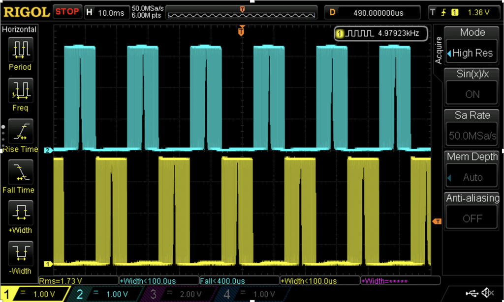
4. Demo:
When you probe both PA0 and PA1 using an oscilloscope, you should get the following:
Happy coding 🙂
3 Comments
Hello,
Thank you very much for your expanation. It’s very helpful guide.
Why Enable ude,tde,cc1de and cc2de when what u actually need is just your ccxde
Hi,
you are correct.
The code was a test code when I accidentally used it rather than the final version.
However, enabling those it irrelevant since they won’t be triggered at all.
Add Comment