TIM1 is an advanced-control timer on STM32 microcontrollers designed for high-performance applications that require precise timing, complementary PWM generation, and robust safety features. This guide explains the key capabilities of TIM1 and demonstrates how to generate synchronized PWM and PWMN signals commonly used in motor control and power electronics.
In this guide, we shall cover the following:
- Introduction.
- STM32CubeMX setup.
- Importing Project to STM32CubeIDE.
- Firmware Development.
- Results.
1. Introduction:
TIM1 is an advanced-control timer available in many STM32 microcontrollers and is specifically designed to address the stringent requirements of high-performance real-time control applications. Unlike general-purpose timers, TIM1 integrates a rich set of hardware features that enable precise waveform generation, deterministic timing behavior, and enhanced safety mechanisms. These capabilities make TIM1 a cornerstone peripheral in systems such as motor drives, power inverters, switched-mode power supplies, and industrial automation platforms, where timing accuracy, phase consistency, and signal integrity are critical.
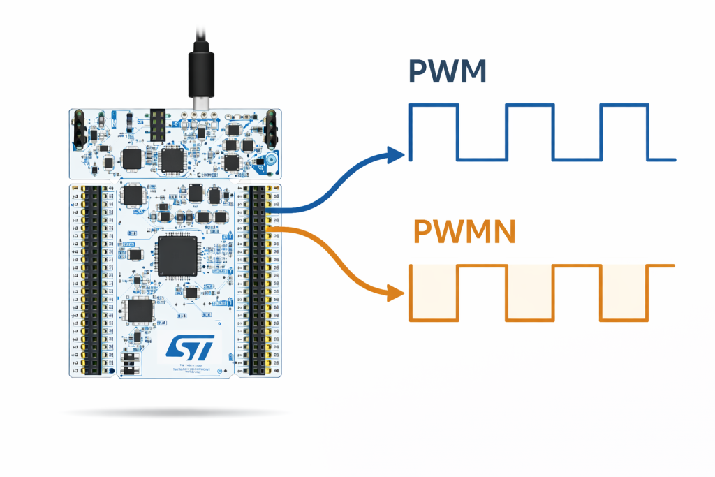
One of the defining features of TIM1 is its ability to generate complementary PWM outputs, commonly referred to as PWM and PWMN signals. These paired outputs are internally synchronized and hardware-inverted versions of each other, allowing direct control of half-bridge or full-bridge power stages without the need for external logic. By providing both the main and complementary signals from a single timer channel, TIM1 significantly simplifies hardware design while ensuring precise, cycle-accurate switching behavior.
Advanced-Control Timer Architecture
TIM1 belongs to the class of advanced-control timers, which distinguishes it from standard 16-bit timers by incorporating additional control logic tailored for power electronics and motion control. These enhancements include complementary output channels, programmable dead-time insertion, break and emergency shutdown inputs, repetition counters, and flexible trigger routing. Together, these features allow TIM1 to safely and efficiently drive power switches such as MOSFETs and IGBTs under demanding electrical and thermal conditions.
The internal architecture of TIM1 ensures that PWM waveforms are generated entirely in hardware. Once configured, the timer autonomously produces stable, repeatable outputs with no CPU intervention, eliminating jitter caused by interrupt latency or software scheduling. This hardware autonomy is essential for maintaining consistent switching patterns, particularly at high PWM frequencies where even small timing variations can result in increased losses, electromagnetic interference, or mechanical vibration in motors.
PWM and Complementary PWMN Concept
In power-stage control, it is often necessary to drive two switching devices in a complementary manner—when one device is on, the other must be off. The PWM/PWMN signal pair fulfills this requirement by producing two outputs that are logically inverted with respect to each other while remaining precisely aligned in time. TIM1 ensures that this inversion is performed internally, guaranteeing exact symmetry and eliminating the risk of software-induced mismatches.
Beyond simple inversion, TIM1 allows both outputs to be synchronously modified in response to duty-cycle changes, frequency updates, or synchronization events. This ensures that the PWM and PWMN signals always maintain their intended relationship, even during dynamic system operation such as speed changes, torque adjustments, or load transitions.
Importance of Dead-Time and Signal Integrity
A critical consideration when using complementary PWM signals is the prevention of shoot-through, a condition where both high-side and low-side switches conduct simultaneously, potentially damaging the power stage. TIM1 addresses this challenge through built-in dead-time insertion, which enforces a programmable delay between the switching of PWM and PWMN outputs. This delay is applied consistently and accurately in hardware, independent of CPU load or execution timing.
The ability to generate PWM and PWMN signals with guaranteed dead-time and precise inversion makes TIM1 especially suitable for safety-critical and high-power systems. It reduces reliance on external gate-driver logic, minimizes component count, and improves overall system reliability.
Applications and Use Cases
The features of TIM1 make it ideal for a wide range of applications, including:
- Three-phase motor control (BLDC, PMSM, induction motors)
- Half-bridge and full-bridge DC-DC converters
- Power inverters and UPS systems
- Digital power control and energy management
- Industrial motion control and robotics
In all these cases, the ability to generate synchronized PWM and PWMN signals with hardware-level precision is fundamental to achieving efficient, stable, and safe system operation.
Why TIM1 Is the Preferred Choice
By combining high-resolution PWM generation, complementary outputs, dead-time control, and safety mechanisms into a single peripheral, TIM1 enables engineers to implement complex control strategies with minimal external circuitry and minimal software complexity. This hardware-centric approach not only improves timing accuracy but also enhances system robustness, scalability, and maintainability.
For these reasons, TIM1 is widely regarded as the primary timer for advanced control tasks in the STM32 ecosystem, and a thorough understanding of its PWM and PWMN capabilities is essential for any engineer working in power electronics or real-time embedded control.
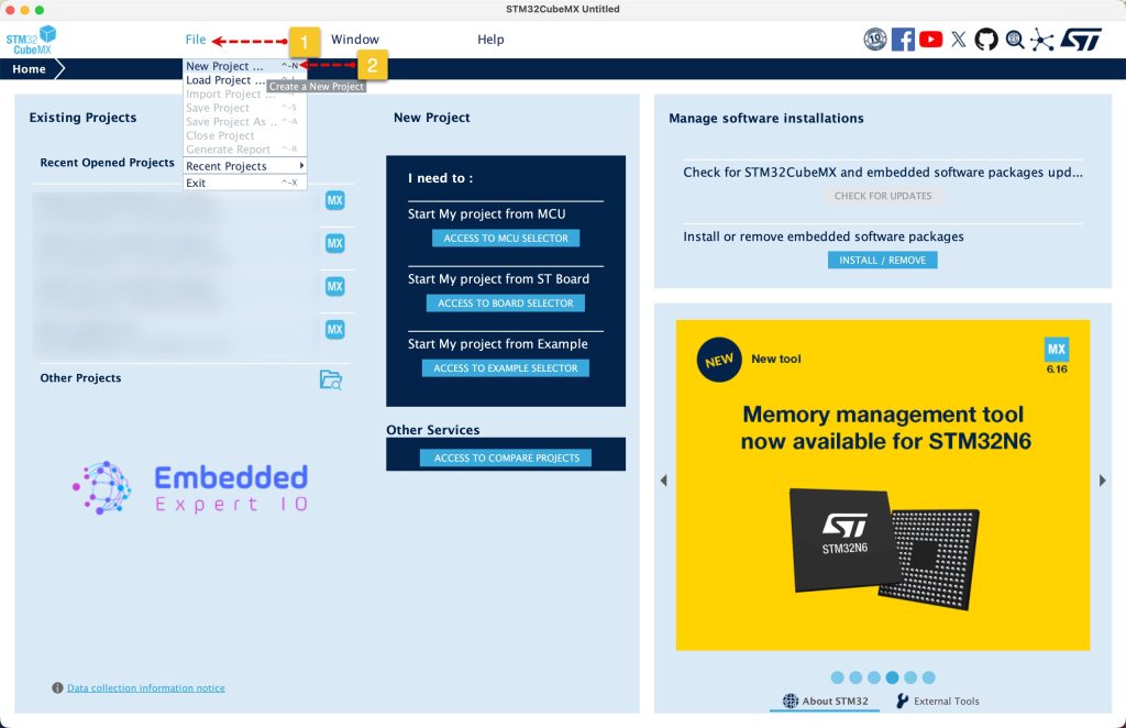
2. STM32CubeMX Setup:
Open STM32CubeMX as start a new project as follows:
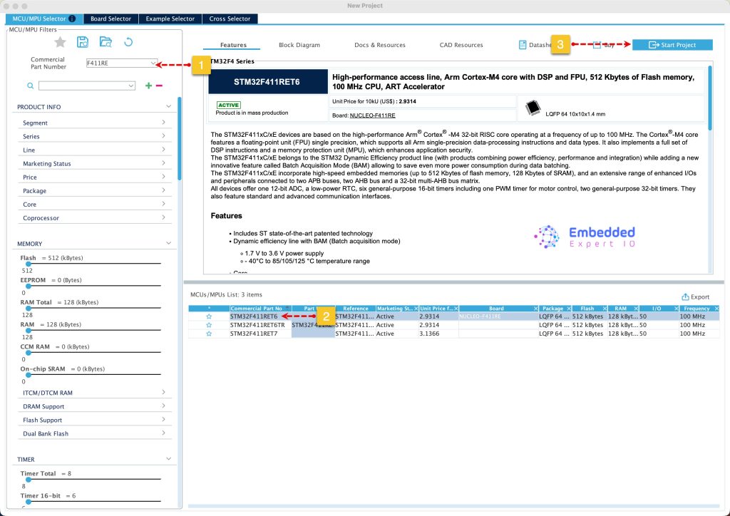
Search for your STM32 MCU, select the MCU and click on Start New Project as follows:
Once the project started, from timers, select TIM1 and set the clock source to be internal and set Channel1 as PWM Generation CH1CH1N as follows
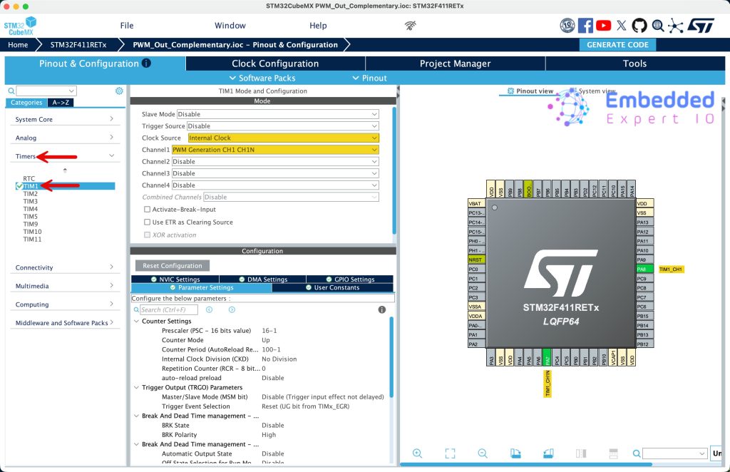
This will configure PA8 and PA7 TIM1_CH1 and TIM1_CH1N respectively.
Next, configure the timer as follows:
- Set Prescaler to 16-1 and Counter Period to 100-1. This will give us 10KHz PWM signal which is typical for most applications.
- Set Pulse to 40-1, this will give us duty cycle of 39% for CH1.

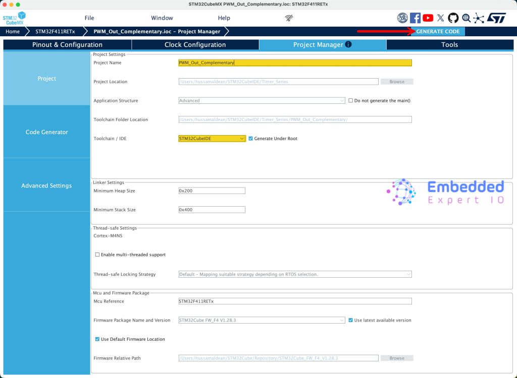
From Project Manager:
Give the project a name, set the location, set toolchain/IDE to STM32CubeIDE and click on Generate Code.
3. Importing the Project to STM32CubeIDE:
Open STM32CubeIDE, select your workspace and click on Launch.
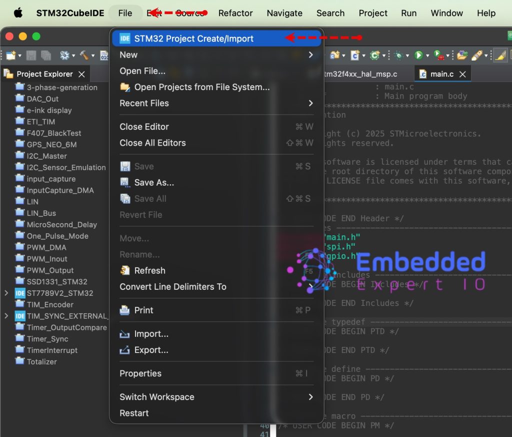
From the IDE, click File and select STM32 Project Create/Import as follows:
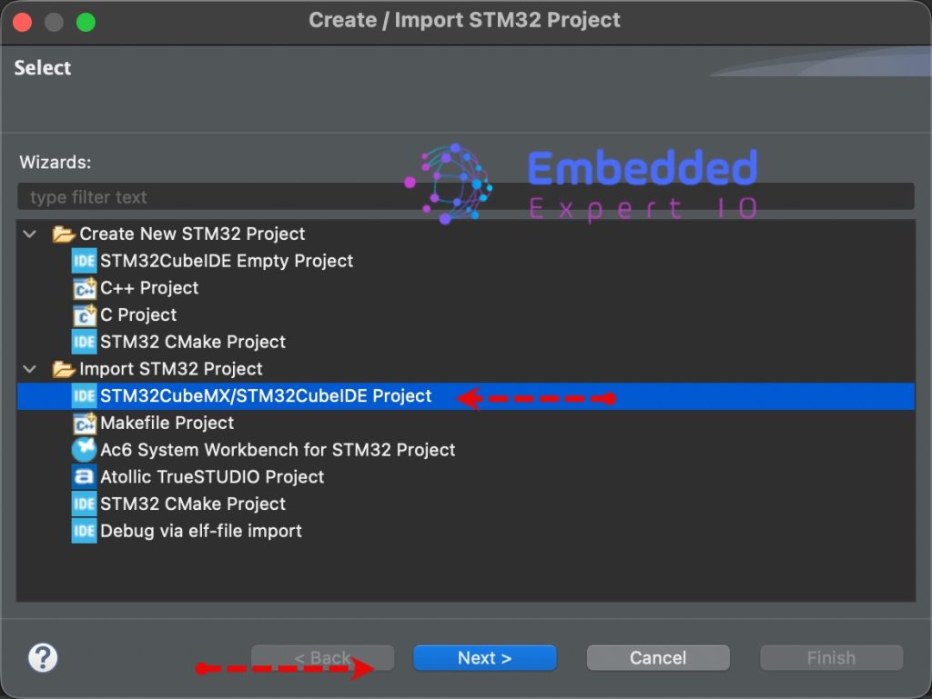
Next, from Import STM32 Project, select STM32CubeMX/STM32CubeIDE Project and click on Next as follows:
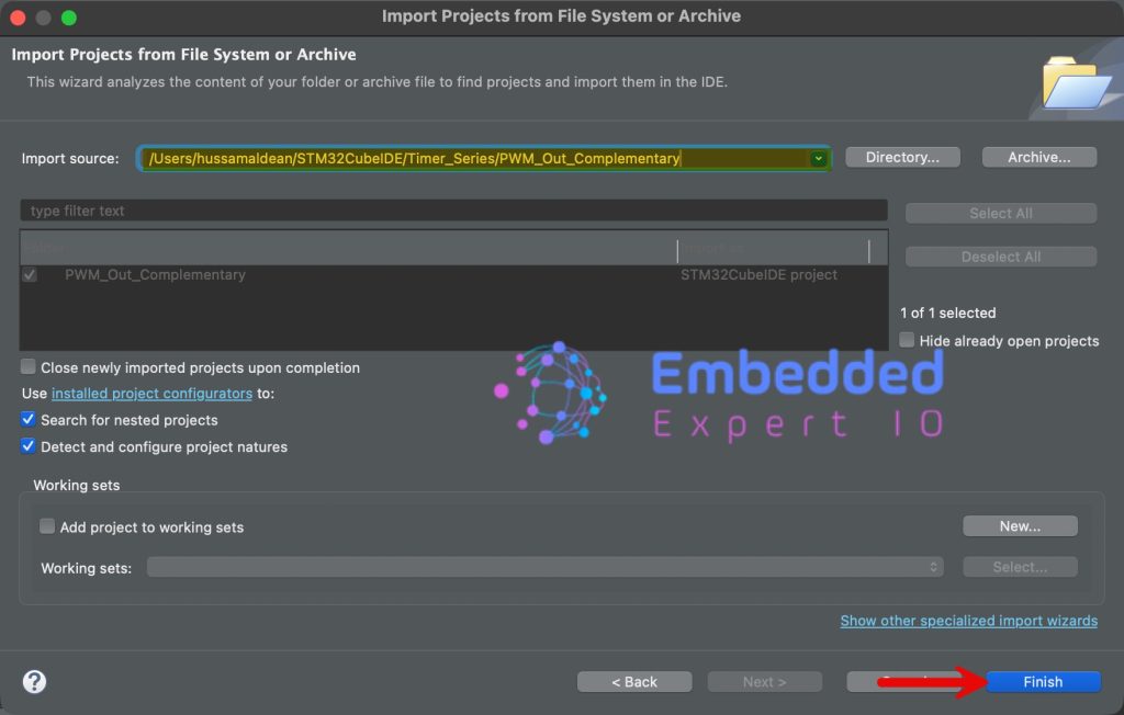
Next, select the folder that contains the .ioc file and click on Finish as follows:
4. Firmware Development:
In main.c file within STM32CubeIDE, in user code begin 2 in main function, start the PWM for TIM1_CH1 as follows:
HAL_TIM_PWM_Start(&htim1,TIM_CHANNEL_1);
Next, start the complementary PWM channel as follows:
HAL_TIMEx_PWMN_Start(&htim1, TIM_CHANNEL_1);
Thats all for the guide, click on run to save the project, build it and flash it as follows:

5. Results:
By probing PA7 and PA8 using logic analyzer or oscilloscope, you will get the following:
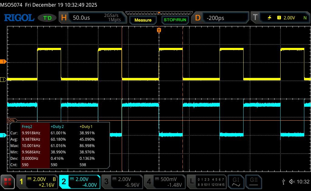
The frequency is 10KHz as aspected from the timer configuration.
Duty cycle of CH1 is 39% as we set it in the configuration (Yellow trace).
Duty cycle of CH1N is 61, which is the remaining of the CH1 off state.
Next, we shall introduce dead time generation.
Stay tuned.
Happy coding 😉
Add Comment