In this guide, we demonstrate how to emulate an SPI-based sensor using two STM32 Nucleo-64 boards—one configured as the SPI master and the other as an emulated SPI sensor. In Part 1, we will discuss the importance of this setup and explain how to configure both the master and slave MCUs for reliable SPI communication.
In this guide, we shall cover the following:
- Introduction.
- Hardware connection.
- Master configuration.
- Slave configuration.
1. Introduction:
In modern embedded systems, the Serial Peripheral Interface (SPI) is one of the most widely used communication protocols for connecting microcontrollers with peripheral devices such as sensors, memory chips, and displays. Its simplicity, high speed, and full-duplex communication make it an ideal choice for applications that require fast and reliable data transfer. However, when developing or testing firmware that depends on SPI-based sensors, engineers often encounter a common challenge: the actual sensor hardware might not be available during early development, or it may be impractical to use due to limited quantities, procurement delays, or environmental constraints. This situation can slow down the entire development process and hinder firmware validation.
To overcome this challenge, an effective approach is to emulate an SPI-based sensor using another STM32 microcontroller. By configuring one STM32 board as an SPI slave that mimics a sensor’s communication behavior, developers can create a controlled environment that allows them to fully test and debug their SPI master firmware without needing the physical sensor. This technique not only accelerates the development process but also provides a flexible platform for simulating a variety of sensor responses and behaviors, such as normal readings, fault conditions, or specific data sequences, enabling comprehensive validation before deployment.
In this project, we will use two STM32 Nucleo-64 boards. One board will function as the SPI master, representing the main controller unit—typically the microcontroller in a real embedded application that communicates with sensors or external peripherals. The second board will serve as the SPI slave, emulating the SPI sensor device. This configuration provides a complete setup for developers to experiment with SPI signaling, synchronization, and data integrity while having full control over both sides of the communication link.
In Part 1, we will discuss in detail the importance of SPI emulation in embedded system development and testing. We will explain how emulating sensors can significantly reduce development time, minimize dependency on hardware availability, and allow firmware engineers to test their SPI drivers in isolation. This method also facilitates easier debugging since the emulated slave MCU can be programmed to provide deterministic and predictable responses, making it easier to trace and analyze the master’s behavior under different conditions.
We will then move on to the configuration of both the master and slave MCUs. This includes setting up the SPI peripheral on both sides—defining the clock polarity (CPOL), clock phase (CPHA), data frame size, bit order (MSB or LSB first), and communication speed. Additionally, we will configure the necessary GPIO pins (SCK, MISO, MOSI, and NSS) to establish a proper physical connection between the two boards. Timing considerations, interrupt usage, and synchronization techniques will also be discussed to ensure stable and accurate data exchange between the master and the emulated sensor.
By the end of this section, you will have a solid understanding of how to prepare and configure both STM32 Nucleo-64 boards for SPI communication. More importantly, you will appreciate the broader purpose of SPI sensor emulation—how it enhances testing efficiency, enables early firmware development, and provides a versatile platform for experimenting with SPI transactions, all before the actual sensor hardware becomes available. This approach represents a practical, powerful, and educational technique that benefits both beginners and experienced embedded engineers alike.
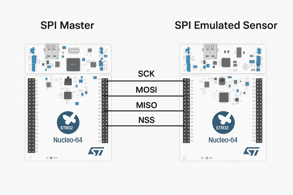
2. Hardware Connection:
The connection as follows:
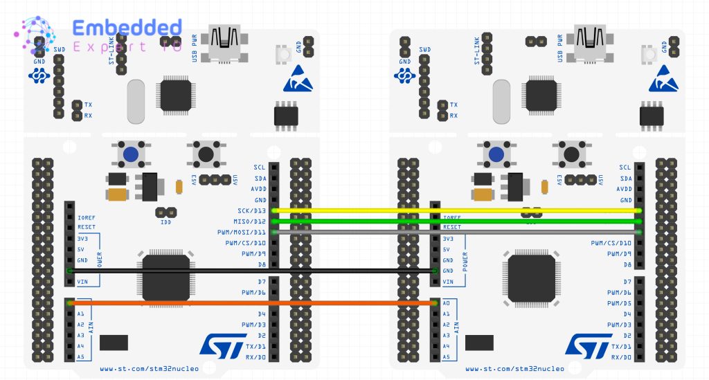
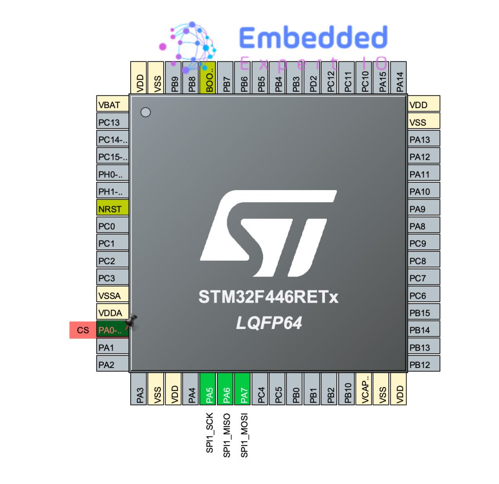
| SPI Pins | Master STM32 | Slave STM32 |
| SCK | PA5 | PA5 |
| MISO | PA6 | PA6 |
| MOSI | PA7 | PA7 |
| SPI CS | PA0 | PA0 |
| — | GND | GND |
3. Master Configuration:
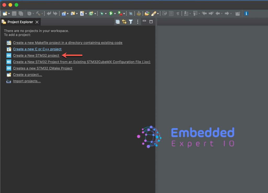
We start off by creating new project as follows:
Open STM32CubeIDE after selecting the workspace and create new project as following:
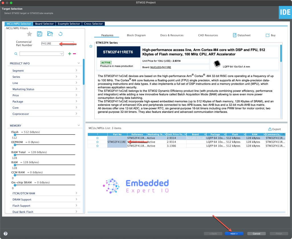
Next, select your MCU and click next as follows:
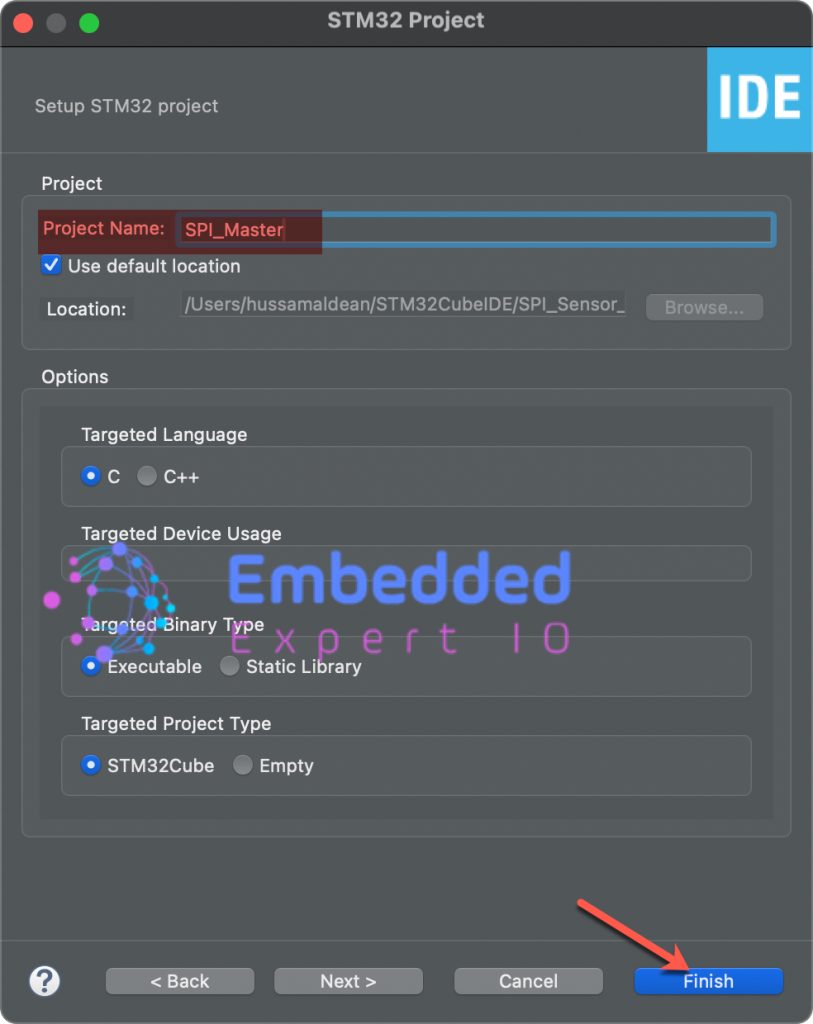
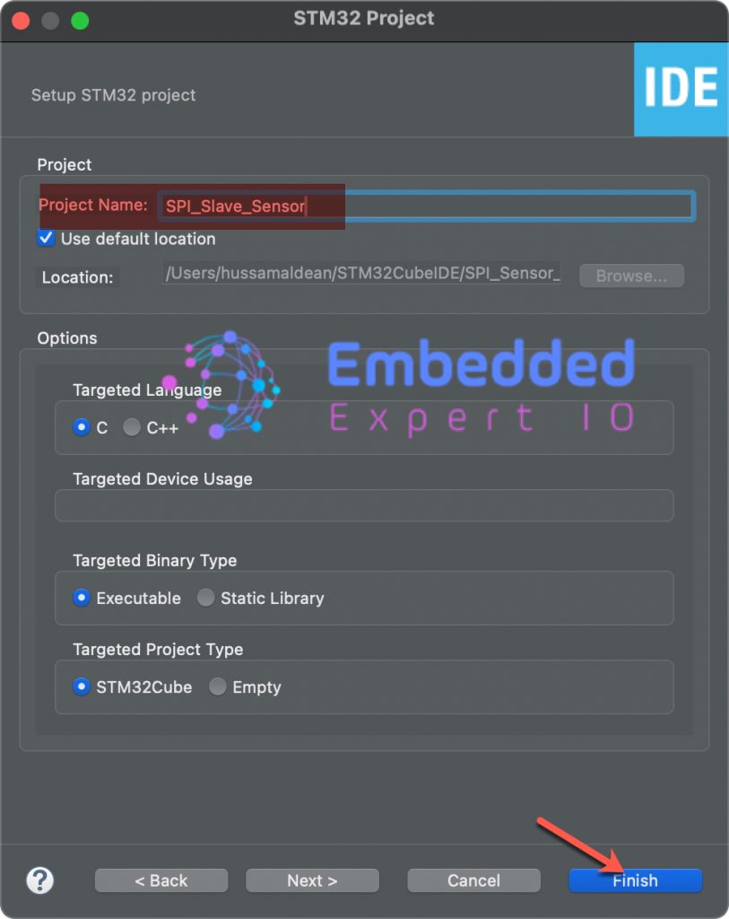
Give the project a name and click on finish as follows:
Once the project has been created, STM32CubeMX window will appear.
From connectivity, Select SPI1 and enable it master full duplex mode as follows:
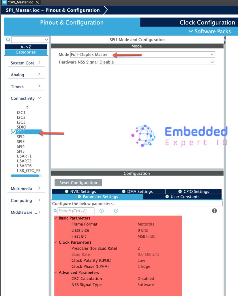
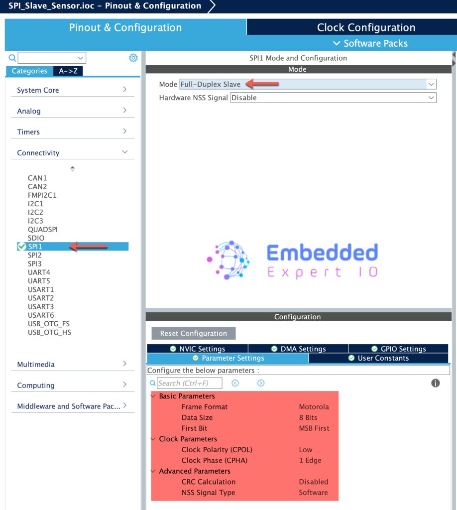
Keep the parameters as is.
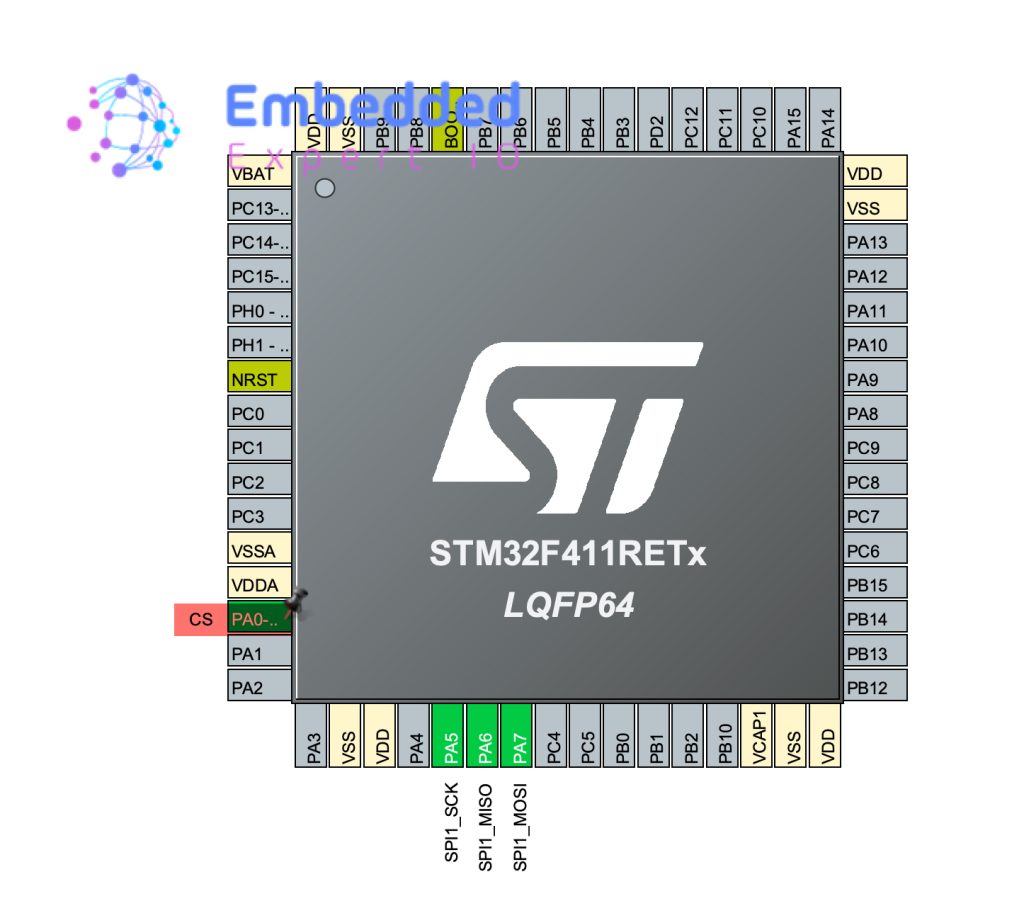
Next, set PA0 as GPIO Output and give it CS name as follows:
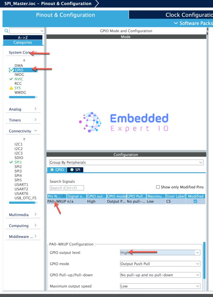
Next, head to system core, GPIO and set PA0 level to high as follows:
Thats all for Master Configuration. Save the project and the code shall be generated.
4. Slave Configuration:
Create a new project and give it a name as follows:
Next, from connectivity, select SPI and set it to Full Duplex Slave as follows:
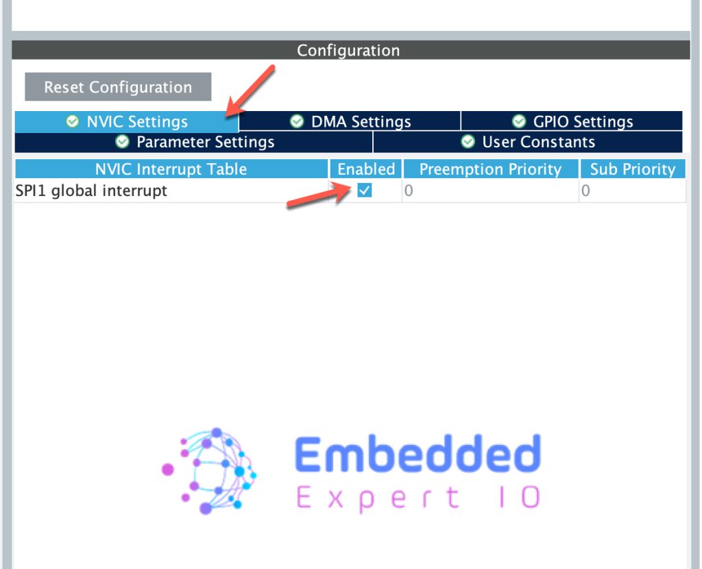
Next, enable SPI interrupts as follows:
Next, Set PA0 as EXTI0 interrupt and give it a name of CS as follows:
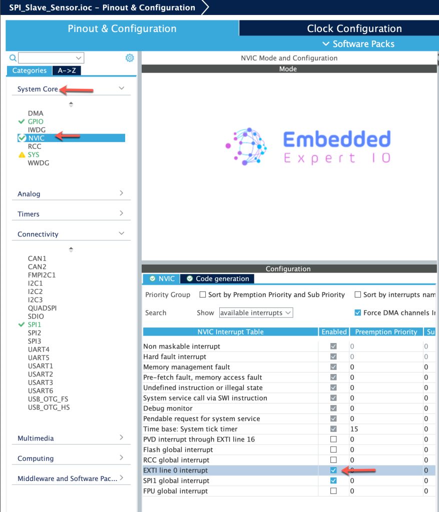
Next, from System Core, NVIC enable EXTI0 line as follows:
Thats all for slave configuration.
Save project and this will generate the code.
In part 2, we shall configure master to transmit data and the slave will receive it.
Stay tuned.
Happy coding 😉
Add Comment