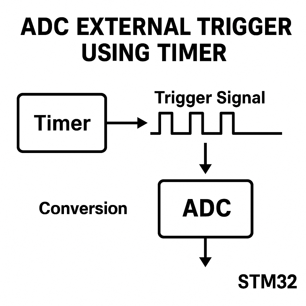
In this part of the STM32 ADC series, we explore how to use external triggers from timers to start ADC conversions automatically. This method enables precise and periodic sampling synchronized with timer events, ideal for real-time control, signal acquisition, and deterministic sampling applications.
In this guide, we shall cover the following:
- Introduction.
- STM32CubeIDE setup.
- Firmware development.
- Results.
1. Introduction:
Introduction to ADC External Trigger Using Timer in STM32
In embedded systems, precise and deterministic sampling of analog signals is essential for real-time monitoring, control, and signal processing. Relying on software-triggered ADC conversions introduces uncertainties due to variable software execution times and interrupt latencies, especially in multitasking environments. To overcome this, STM32 microcontrollers offer the capability to use external triggers, particularly from internal timers, to initiate ADC conversions at exact intervals with minimal jitter.
What is an External Trigger?
An external trigger for ADC is a hardware event or signal that instructs the ADC to start a conversion without CPU intervention. While “external” often refers to external pins, STM32 also allows internal peripherals, such as timers, to act as trigger sources. This mechanism is invaluable in applications requiring:
- Periodic sampling at fixed frequencies (e.g. data loggers, sensor acquisition).
- Synchronized sampling with PWM signals in motor control and power conversion systems.
- Real-time signal processing, where sampling period consistency directly affects accuracy (e.g. FFT or digital filters).
- Reduced CPU load, since timers autonomously generate the trigger without software polling or manual triggering.
How Does Timer Trigger Work?
When configured, a timer output event (such as an update event, compare match, or PWM edge) is routed internally as the ADC’s external trigger input. Upon receiving this event, the ADC immediately begins its sampling and conversion process. The timer continues counting based on its configuration, generating periodic triggers at precise intervals determined by the system clock and timer prescaler settings.
Key Benefits
- Deterministic Sampling Interval: Hardware triggers ensure each ADC conversion starts at exactly the intended time, essential for time-domain signal integrity.
- Minimal Jitter: Unlike software-triggered conversions, timer-based triggering has negligible timing jitter, improving measurement accuracy.
- Offloading the CPU: The CPU does not need to manage conversion timing manually, freeing it for data processing or other tasks.
- Synchronization with Other Peripherals: In motor control, the ADC can sample current precisely aligned with PWM cycles to implement effective closed-loop control.
Practical Example Applications
- Motor Control (FOC, BLDC): Sampling phase currents synchronised to PWM cycles.
- Digital Oscilloscope or Data Logger: Acquiring voltage signals at uniform sample rates for plotting or storage.
- Power Monitoring: Sampling voltage and current waveforms synchronised with grid frequency or inverter switching.
2. STM32CubeIDE Setup:
Once you started a new project, enable ADC CH1 as follows:
- IN1 as single ended (Not all STM32 MCUs have this feature).
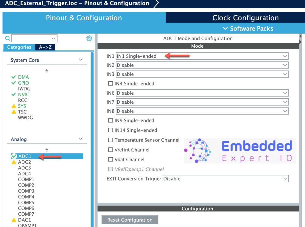
Next, in Parameters Settings:
- Set DMA Continuous Requests to Enabled.
- External Trigger Conversion Source to Timer 3 Trigger Out event.
- External Trigger Edge to rising edge.

Note: In case you have selected capture compare event, select the edge to be both, rising and falling edge.
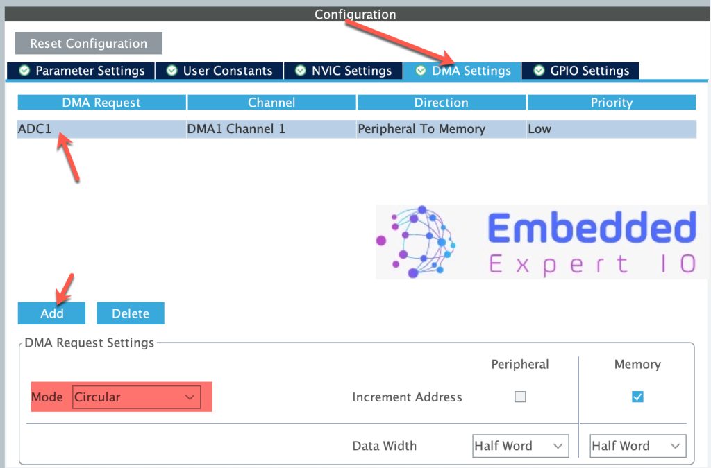
Next, DMA Settings tab, configure the DMA as follows:
- Add DMA for ADC1.
- Set the mode to Circular.
- Data Width to half word (16-bit).
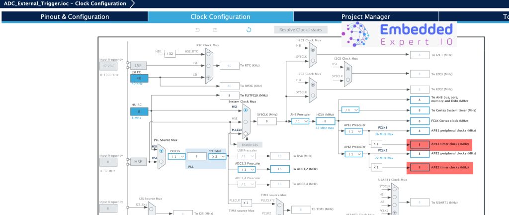
Next, before we configure the timer, we need to find the timer frequency, from Clock Configuration:
Note the APB1 and APB2 timer clocks, in this case is 8MHz since the default frequency for STM32F303 is 8MHz.
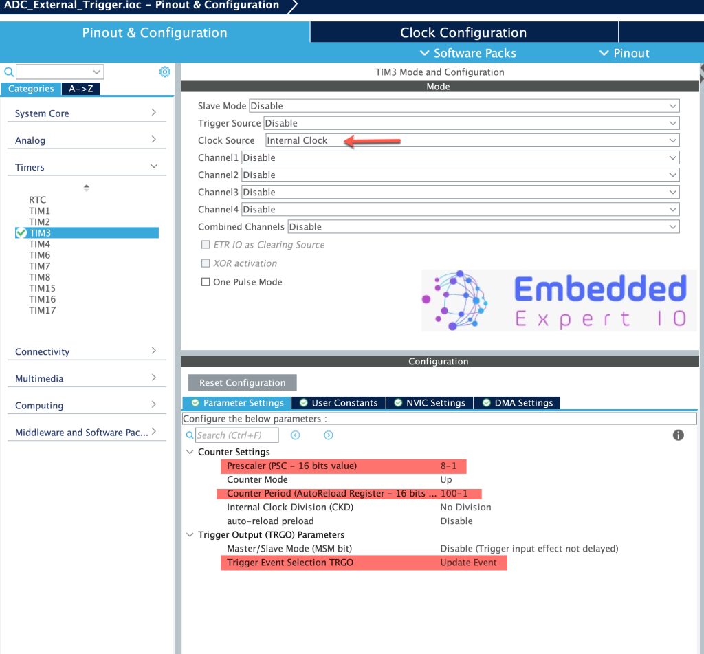
Next, we shall configure TIM3 as follows:
- Clock Source to Internal Clock.
- Prescaler to 8-1 (The timer now is operating at 1MHz).
- Counter Period to 100-1. The timer shall overflow each 100uS.
- Set Trigger event Selection to Update Event.
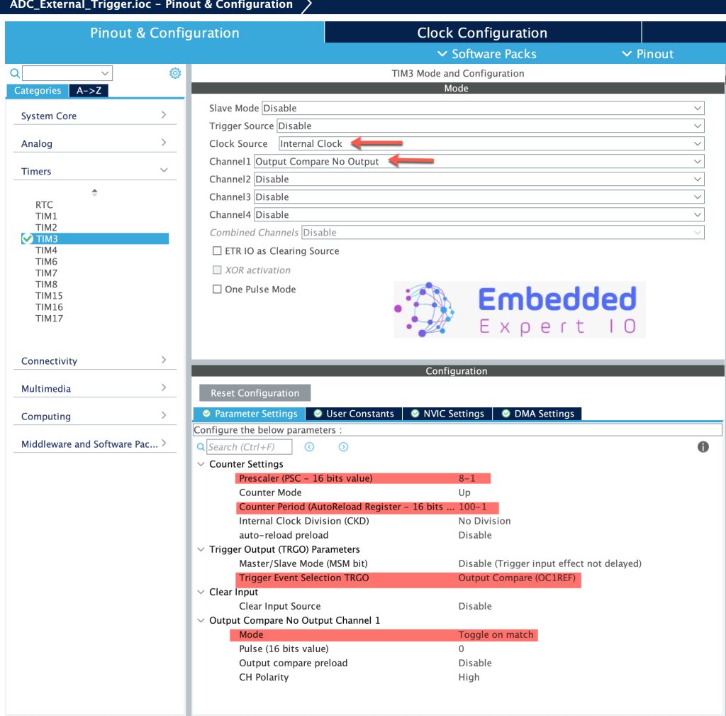
In case you have select capture compare event:
- Set the required channel to Output Compare No Output.
- Trigger Event Selection to Output Compare (OCxREF), where x is the channel number.
- Set channel mode to be Toggle on Match.
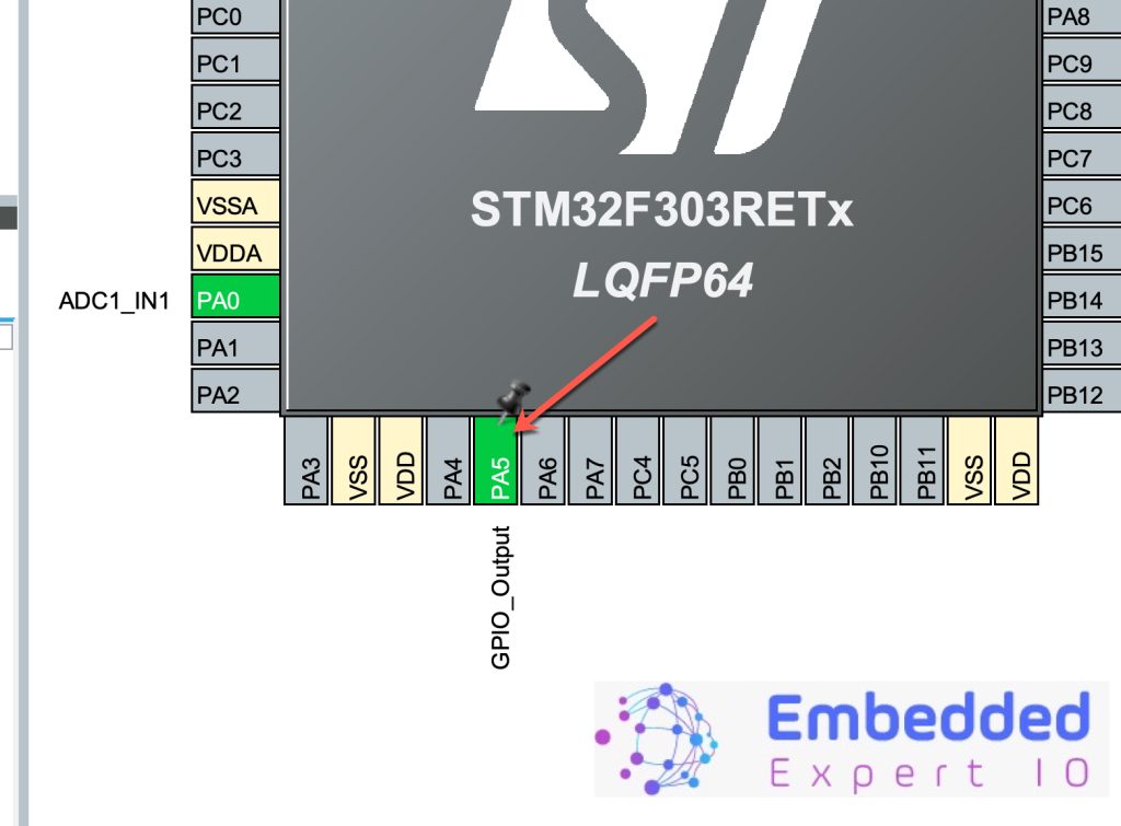
Also, enable any pin as GPIO output (Here we are using PA5):
Thats all for the configuration. Save the project and this will generate the project.
3. Firmware Development:
After the code has been generated, main.c will be opened.
In main.c in user code begin PV, declare the following variable to hold the ADC value as follows:
uint16_t ADC_VAL[1];
In user code begin 0, declare the following function:
void HAL_ADC_ConvCpltCallback(ADC_HandleTypeDef *hadc)
{
  HAL_GPIO_TogglePin(GPIOA, GPIO_PIN_5);
}
This function shall be called every time ADC finishes conversion.
In user code begin 2, start the ADC in DMA mode and the timer in base mode as follows:
  HAL_TIM_Base_Start(&htim3);
  HAL_ADC_Start_DMA(&hadc1, (uint32_t)&ADC_VAL, 1);
Thats all for the firmware, save the project and start a debugging session.

4. Results:
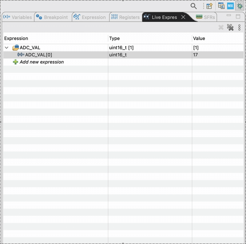
By adding ADC_VAL to Live expression, you should get the following:
By probing PA5 or the pin you selected, you should notice the following:
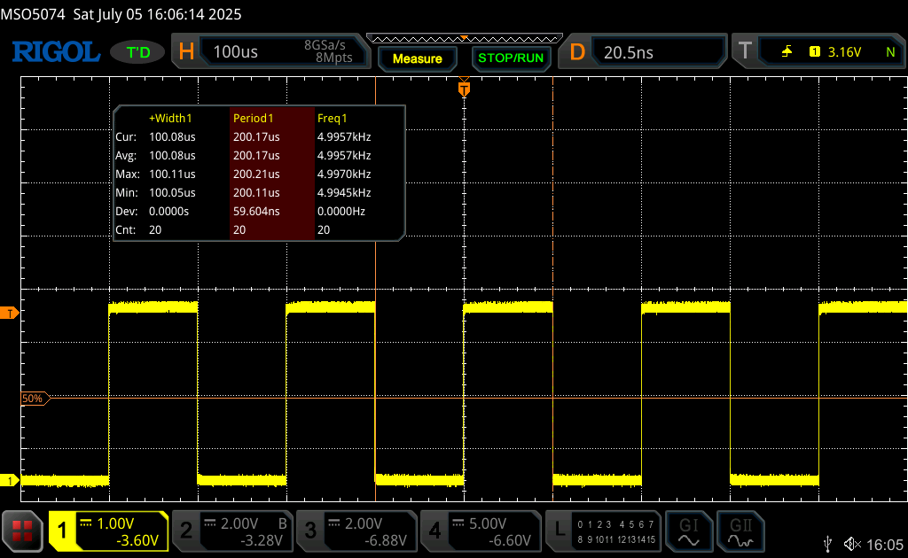
Notice the +width and -width of the signal, they are 100uS. Thats means the ADC is triggered every 100uS which is according to the timer setup.
Happy coding 😉
Add Comment