
In the pervious guide (here), we saw how to send data over SPI using DMA. In this guide, we shall communicate with slave device (MPU9250 in this case) to read the acceleration part.
In this guide, we shall cover the following:
- Send multiple data function.
- Configure SPI to receive data.
- Receive data function.
- MPU9250 connection.
- MPU9250 code.
- Main code.
- Results.
1. Send Multiple Data Function:
Before sending multiple data, visit this guide to have an idea what is SPI and how to configure it.
We start by creating new source and header files with name of SPI1.c and SPI1.h respectively.
In the header file:
Include the header guard as following:
#ifndef SPI1_H_
#define SPI1_H_


#endif /* SPI1_H_ */
Within the header guard, include stdint library as following:
#include "stdint.h"
Declare the following functions:
void SPI1_Pins_Init(void);
This function shall initialize SPI related pins and it takes no argument and returns nothing.
void SPI1_Init(void);
This function will initialize SPI1 and it takes no argument and returns nothing.
void SPI1_TX (uint8_t *data,uint16_t len);
This function will transmit data over SPI bus and takes pointer to data array and the length of the data to be transferred.
void SPI1_RX (uint8_t *data, uint8_t len);
This function will read the SPI bus and takes pointer to the array where the data shall be stored and number of the data to be read.
Hence, the header file as following:
#ifndef SPI1_H_
#define SPI1_H_


#include "stdint.h"

void SPI1_Pins_Init(void);
void SPI1_Init(void);
void SPI1_TX (uint8_t *data,uint16_t len);
void SPI1_RX (uint8_t *data, uint8_t len);

#endif /* SPI1_H_ */
For the source file:
GPIO initialization:
Include the following header file:
#include <SPI1.h>
#include "stm32f7xx.h"
For GPIO initialization:
void SPI1_Pins_Init(void)
{

	//enable clock for GPIOA
	RCC->AHB1ENR|=RCC_AHB1ENR_GPIOAEN;

	//set PA5, PA6 and PA7 to alternate function mode
	GPIOA->MODER|=GPIO_MODER_MODER5_1|GPIO_MODER_MODER6_1|GPIO_MODER_MODER7_1;

	GPIOA->MODER&=~(GPIO_MODER_MODER5_0|GPIO_MODER_MODER6_0|GPIO_MODER_MODER7_0);

	#define AF05 0x05

	GPIOA->AFR[0]|=(AF05<<GPIO_AFRL_AFRL5_Pos)|(AF05<<GPIO_AFRL_AFRL6_Pos)|(AF05<<GPIO_AFRL_AFRL7_Pos);


}
For SPI initialization:
he SPI configuration as following:

In Control Register 1 (CR1):
- Enable Clock access to SPIIBaud to be Fclk/2 (according to your application).
- CPOL and CPHA to 1 (according to your application also).
- Full duplex mode.
- Master Mode.
- Software slave management.
In CR2, set the length to be 8-bit:

void SPI1_Init(void)
{
	//enable clock access to SPI1
	RCC->APB2ENR|=RCC_APB2ENR_SPI1EN;

	//software slave management
	SPI1->CR1|=SPI_CR1_SSM|SPI_CR1_SSI;

	// set SPI as master mode
	SPI1->CR1|=SPI_CR1_MSTR;

	/*Set CPOL to 1 and CPHA to 1*/
	SPI1->CR1 |=SPI_CR1_CPOL;
	SPI1->CR1 |=SPI_CR1_CPHA;

	/*Set data size to 8-bit*/
	SPI1->CR2&=~(SPI_CR2_DS_Msk);
	SPI1->CR2|=(0x07<<SPI_CR2_DS_Pos);


	/*Enable SPI peripheral*/
	SPI1->CR1|=SPI_CR1_SPE;
}
To send multiple bytes, we shall use the following function:
void SPI1_TX(uint8_t *data,uint16_t len)
{
	uint32_t i=0;
	while(i<len)
	{
		/*Wait until TXE is set*/
		while(!(SPI1->SR & (SPI_SR_TXE)))
		{}

		/*Write the data to the data register*/
		*((volatile uint8_t *)&SPI1->DR) = data[i];
		i++;
	}
	/*Wait until TXE is set*/
	while(!(SPI1->SR & (SPI_SR_TXE))){}

	/*Wait for BUSY flag to reset*/
	while((SPI1->SR & (SPI_SR_BSY))){}

	/*Clear OVR flag*/
	(void)SPI1->DR;
	(void)SPI1->SR;
}
First, declare a local variable i, then similar to sending single character, we shall send the array byte by byte.
Thats all for the sending part.
2. Configure SPI to Receive Data:
Since the SPI is already configured in full duplex mode, it has the ability to receive data. However, since the data to received is 8-bit long, we need to configure the FIFO threshold in CR2 as following:


Hence, we shall add this line to the initialization function:
	/*Set FIFO to be 1/4 */
	SPI1->CR2|=SPI_CR2_FRXTH;
Thats all for the SPI configuration.
3. Receive Data Function:
In order to receive data, we shall do the following steps:
- Iterate for the length of the data to be read.
- Within the iteration, send dummy data then wait until the RXNE (Receive buffer not empty) is set then read the data register.
void SPI1_RX (uint8_t * data, uint8_t len)
{

	while(len)
	{
		/*Send dummy data*/
		*((volatile uint8_t *)&SPI1->DR) =0x00;

		/*Wait for RXNE flag to be set*/
		while(!(SPI1->SR & (SPI_SR_RXNE))){}

		/*Read data from data register*/
		*data++ =SPI1->DR;
		len--;
	}

}
Hence, the source file as following:
#include <SPI1.h>
#include "stm32f7xx.h"


void SPI1_Pins_Init(void)
{

	//enable clock for GPIOA
	RCC->AHB1ENR|=RCC_AHB1ENR_GPIOAEN;

	//set PA5, PA6 and PA7 to alternate function mode
	GPIOA->MODER|=GPIO_MODER_MODER5_1|GPIO_MODER_MODER6_1|GPIO_MODER_MODER7_1;

	GPIOA->MODER&=~(GPIO_MODER_MODER5_0|GPIO_MODER_MODER6_0|GPIO_MODER_MODER7_0);

	#define AF05 0x05

	GPIOA->AFR[0]|=(AF05<<GPIO_AFRL_AFRL5_Pos)|(AF05<<GPIO_AFRL_AFRL6_Pos)|(AF05<<GPIO_AFRL_AFRL7_Pos);


}


void SPI1_Init(void)
{
	//enable clock access to SPI1
	RCC->APB2ENR|=RCC_APB2ENR_SPI1EN;

	//software slave management
	SPI1->CR1|=SPI_CR1_SSM|SPI_CR1_SSI;

	// set SPI as master mode
	SPI1->CR1|=SPI_CR1_MSTR;

	/*Set CPOL to 1 and CPHA to 1*/
	SPI1->CR1 |=SPI_CR1_CPOL;
	SPI1->CR1 |=SPI_CR1_CPHA;

	/*Set data size to 8-bit*/
	SPI1->CR2&=~(SPI_CR2_DS_Msk);
	SPI1->CR2|=(0x07<<SPI_CR2_DS_Pos);

	/*Set FIFO to be 1/4 */
	SPI1->CR2|=SPI_CR2_FRXTH;


	/*Enable SPI peripheral*/
	SPI1->CR1|=SPI_CR1_SPE;
}


void SPI1_TX(uint8_t *data,uint16_t len)
{
	uint32_t i=0;
	while(i<len)
	{
		/*Wait until TXE is set*/
		while(!(SPI1->SR & (SPI_SR_TXE)))
		{}

		/*Write the data to the data register*/
		*((volatile uint8_t *)&SPI1->DR) = data[i];
		i++;
	}
	/*Wait until TXE is set*/
	while(!(SPI1->SR & (SPI_SR_TXE))){}

	/*Wait for BUSY flag to reset*/
	while((SPI1->SR & (SPI_SR_BSY))){}

	/*Clear OVR flag*/
	(void)SPI1->DR;
	(void)SPI1->SR;
}

void SPI1_RX (uint8_t * data, uint8_t len)
{

	while(len)
	{
		/*Send dummy data*/
		*((volatile uint8_t *)&SPI1->DR) =0x00;

		/*Wait for RXNE flag to be set*/
		while(!(SPI1->SR & (SPI_SR_RXNE))){}

		/*Read data from data register*/
		*data++ =SPI1->DR;
		len--;
	}

}
4. MPU9250 Connection:
The connection as following:

| MPU9250 | STM32F767Zi Nucleo-144 |
| Vcc | 5V |
| GND | GND |
| SCL | SCK (PA5) |
| SDA | MOSI |
| AD0 | MISO |
| NCS | PA3 (as chip select) |
5. MPU9250 Code:
Create new source and header files with name of MPU9250.c and MPU9250.h respectively.
Within the header file:
#ifndef __MPU9250__H__
#define __MPU9250__H__


#include "SPI1.h"
#define Pi 3.14159
#define MPU9250_ADDRESS_AD0_LOW  0x68
#define MPU9250_ADDRESS_AD0_HIGH 0x69

#define ACC_FULL_SCALE_2_G       0x00
#define ACC_FULL_SCALE_4_G       0x08
#define ACC_FULL_SCALE_8_G       0x10
#define ACC_FULL_SCALE_16_G      0x18

#define GYRO_FULL_SCALE_250_DPS   0x00
#define GYRO_FULL_SCALE_500_DPS   0x08
#define GYRO_FULL_SCALE_1000_DPS  0x10
#define GYRO_FULL_SCALE_2000_DPS  0x18
#define USER_CTRL									0x6A
#define MAG_MODE_POWERDOWN        0x0
#define MAG_MODE_SINGLE           0x1
#define MAG_MODE_CONTINUOUS_8HZ   0x2
#define MAG_MODE_EXTERNAL         0x4
#define MAG_MODE_CONTINUOUS_100HZ 0x6
#define MAG_MODE_SELFTEST         0x8
#define MAG_MODE_FUSEROM          0xF
#define AK8963_ADDRESS  0x0C
#define AK8963_RA_HXL   0x03
#define AK8963_RA_CNTL1 0x0A
#define AK8963_RA_ASAX  0x10

#define MPU9250_ADDR_ACCELCONFIG  0x1C
#define MPU9250_ADDR_INT_PIN_CFG  0x37
#define MPU9250_ADDR_ACCEL_XOUT_H 0x3B
#define MPU9250_ADDR_GYRO_XOUT_H  0x43
#define MPU9250_ADDR_PWR_MGMT_1   0x6B
#define MPU9250_ADDR_WHOAMI       0x75


void MPU9250_CS_Init(void);
void MPU9250_beginAccel(uint8_t mode);
uint8_t MPU9250_accelUpdate(void);
float MPU9250_accelX(void);
float MPU9250_accelY(void);
float MPU9250_accelZ(void);


#endif
Within the source file:
#include <math.h>
#include "MPU9250.h"

#include "stm32f7xx.h"
uint8_t data[2];

float accelRange,gyroRange;

#define READ_FLAG   0x80

uint8_t accelBuf[6];

uint8_t data[2];


#define CS_LOW()	GPIOA->BSRR=GPIO_BSRR_BR3;
#define CS_HIGH()	GPIOA->BSRR=GPIO_BSRR_BS3;


void MPU9250_CS_Init(void)
{

	RCC->AHB1ENR|=RCC_AHB1ENR_GPIOAEN;

	GPIOA->MODER|=GPIO_MODER_MODER3_0;
	GPIOA->MODER&=~GPIO_MODER_MODER3_1;

	GPIOA->BSRR=GPIO_BSRR_BS3;

}


void MPU9250_beginAccel(uint8_t mode) {
  switch(mode) {
  case ACC_FULL_SCALE_2_G:
    accelRange = 2.0;
    break;
  case ACC_FULL_SCALE_4_G:
    accelRange = 4.0;
    break;
  case ACC_FULL_SCALE_8_G:
    accelRange = 8.0;
    break;
  case ACC_FULL_SCALE_16_G:
    accelRange = 16.0;
    break;
  default:
    return; // Return without writing invalid mode
  }

	data[0]=USER_CTRL; data[1]=(1<<4);
	CS_LOW();
	SPI1_TX(data,2);
	CS_HIGH();

	data[0]=MPU9250_ADDR_ACCELCONFIG; data[1]=mode;
	CS_LOW();
	SPI1_TX(data,2);
	CS_HIGH();

}

uint8_t MPU9250_accelUpdate(void) {

	data[0]=(uint8_t)(0x3B|READ_FLAG);
	CS_LOW();
	SPI1_TX(data,1);
	SPI1_RX((uint8_t*)(accelBuf),6);
	CS_HIGH();

	return 0;
}


float MPU9250_accelGet(uint8_t highIndex, uint8_t lowIndex) {
  int16_t v = ((int16_t) accelBuf[highIndex]) << 8 | accelBuf[lowIndex];
  return ((float) -v) * accelRange / (float) 0x8000; // (float) 0x8000 == 32768.0
}


float MPU9250_accelX(void) {
  return MPU9250_accelGet(1, 2);
}

float MPU9250_accelY(void) {
  return MPU9250_accelGet(3, 4);
}

float MPU9250_accelZ(void) {
  return MPU9250_accelGet(5, 6);
}
6. Main code:
In main.c:
#include "SPI1.h"
#include "MPU9250.h"
#include "stm32f7xx.h"
float acc_x,acc_y,acc_z;

int main(void)
{
	/*Enable float point*/
	SCB->CPACR |= ((3UL << 10*2)|(3UL << 11*2));


	SPI1_Pins_Init();
	SPI1_Init();
	MPU9250_CS_Init();
	MPU9250_beginAccel(ACC_FULL_SCALE_16_G);


	while(1)
	{
		MPU9250_accelUpdate();
		acc_x=MPU9250_accelX();
		acc_y=MPU9250_accelY();
		acc_z=MPU9250_accelZ();
		for (int j=0;j<100000;j++);
	}


}
7. Results
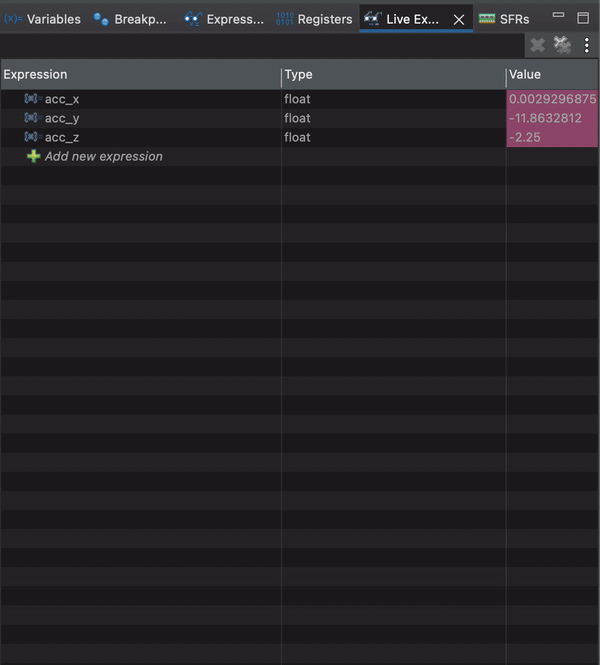
Upload the code to your board and connect the MPU9250, start a debug session and add the acc_x, acc_y and acc_z to live expression
You should see the values changes as following:
Happy coding 🙂
Add Comment