
In this guide, we shall see what is the comparator peripheral and how in general the comparator works.
In this guide, we shall cover the following:
- What is a comparator.
- Comparator peripheral in STM32L053.
- Developing the driver.
- Connection.
- Code.
- Results.
1.1 What is Comparator:
A comparator is an electronic circuit, which compares the two inputs that are applied to it and produces an output. The output value of the comparator indicates which of the inputs is greater or lesser. Please note that comparator falls under non-linear applications of ICs.
An op-amp consists of two input terminals and hence an op-amp based comparator compares the two inputs that are applied to it and produces the result of comparison as the output. This chapter discusses about op-amp based comparators.
1.2 Types of Comparators
Comparators are of two types : Inverting and Non-inverting. This section discusses about these two types in detail.
Inverting Comparator
An inverting comparator is an op-amp based comparator for which a reference voltage is applied to its non-inverting terminal and the input voltage is applied to its inverting terminal. This comparator is called as inverting comparator because the input voltage, which has to be compared is applied to the inverting terminal of op-amp.
The circuit diagram of an inverting comparator is shown in the following figure.
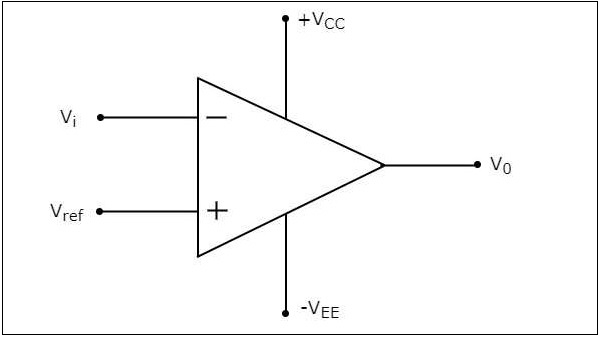
The operation of an inverting comparator is very simple. It produces one of the two values, +Vsat and −Vsat at the output based on the values of its input voltage Vi and the reference voltage Vref. (source).
2. Comparator Peripheral in STM32L053:
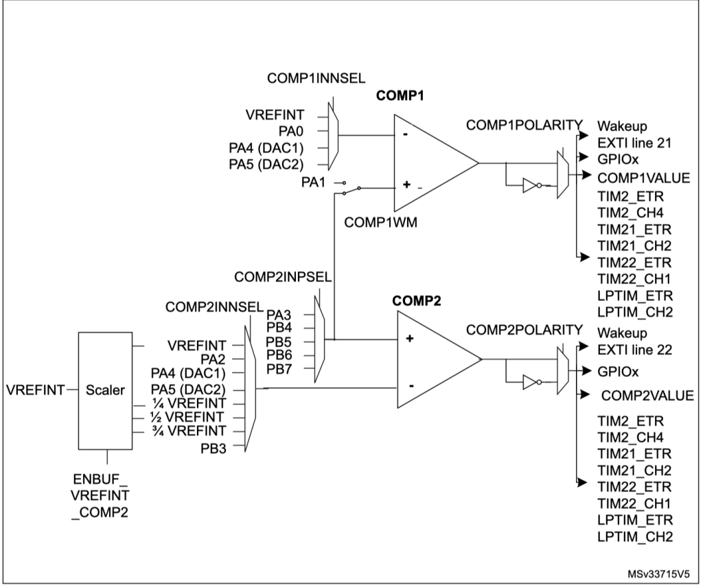
STM32L0x3 devices embed two ultra-low-power comparators COMP1, and COMP2 that can be used either as standalone devices (all terminal are available on I/Os) or combined with the timers.
The comparators can be used for a variety of functions including:
• Wakeup from low-power mode triggered by an analog signal,
• Analog signal conditioning,
• Cycle-by-cycle current control loop when combined with the DAC and a PWM output from a timer.
COMP main features
• COMP1 comparator with ultra low consumption
• COMP2 comparator with rail-to-rail inputs, fast or slow mode
• Each comparator has positive and configurable negative inputs used for flexible voltage selection:
– I/O pins
– DAC
– Internal reference voltage and three submultiple values (1/4, 1/2, 3/4) provided by scaler (buffered voltage divider)
• Programmable speed / consumption (COMP2 only)
• The outputs can be redirected to an I/O or to timer inputs for triggering:
– Capture events
• COMP1, and COMP2 can be combined in a window comparator. Each comparator has interrupt generation capability with wakeup from Sleep and Stop modes (through the EXTI controller)
3. Developing the Driver:
Before we start developing the driver, we need to find which bus the comparator is connected to. We can find this in the datasheet of STM32L053:
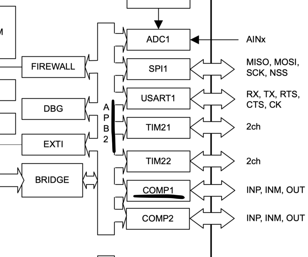
From the block diagram, we can find that COMP1 and COMP2 are being clocked by APB2 bus.
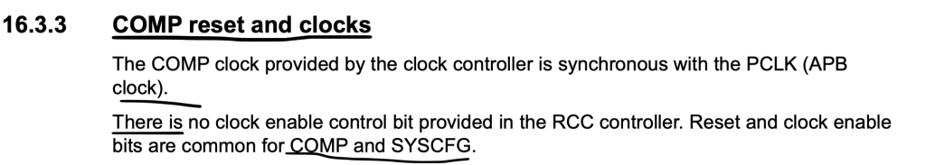
However, in the reference manual of STM32L052, comparator section, it mentioned that COMP1 and COMP2 are being clocked at the same time with SYSCNFG:
Also, the COMP1 has the ability to get the analog signals from PA0 and PA1.
Hence, we shall first set PA0 and PA1 as analog mode:
	/*Enable clock access to GPIOA*/
	RCC->IOPENR |= RCC_IOPENR_GPIOAEN;

	/*Set PA0 and PA1 as analog Mode*/

	GPIOA->MODER|=GPIO_MODER_MODE0|GPIO_MODER_MODE1;
Since we need an output of the comparator, we need to find which pin is connected to COMP1.
We can find that from Alternate function port A table in the datasheet:
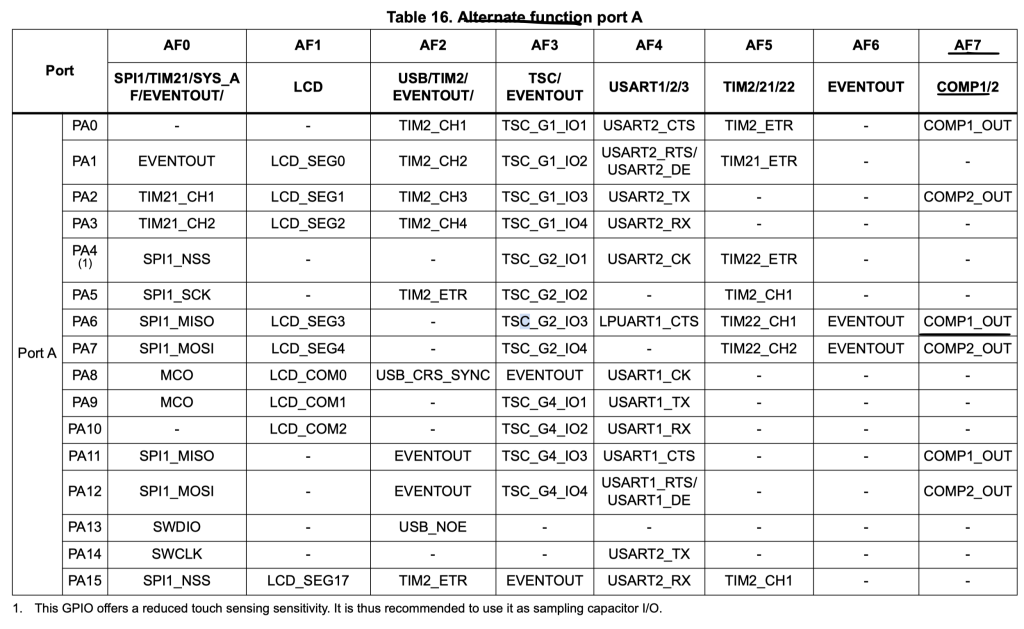
Since PA0 and PA1 are being used by the comparator, we shall use PA6 for the comparator output:
	/*Set PA6 to alternate function*/

	GPIOA->MODER|=GPIO_MODER_MODE6_1;
	GPIOA->MODER&=~GPIO_MODER_MODE6_0;

	/*Set PA6 AF to AF7*/
	#define AF07	7
	GPIOA->AFR[0]|=(AF07<<GPIO_AFRL_AFSEL6_Pos);
Now we can configure the comparator:
Enable clock access to SYSCNFG:
	/*Enable clock access to COMP1 (Same as SYSCFG)*/
	RCC->APB2ENR|=RCC_APB2ENR_SYSCFGEN;
Set the window pin to be PA1:
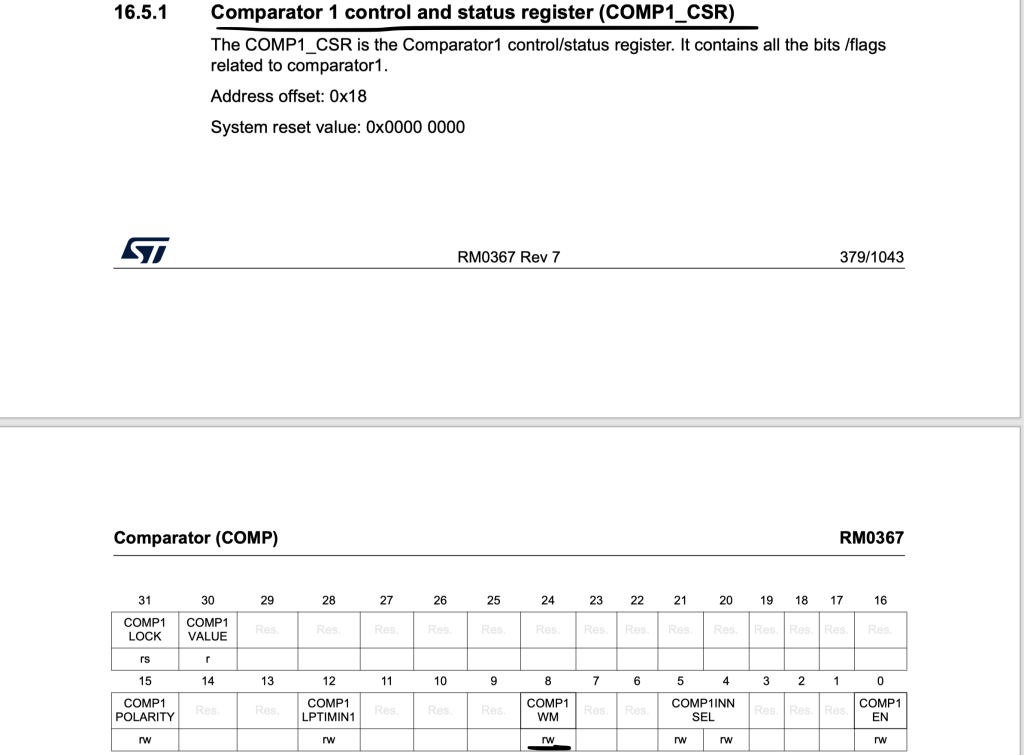

	/*Set the window pin to be PA1*/
	COMP1->CSR&=~ COMP_CSR_COMP1WM;
Set the minus pin to be PA0:

	/*Set the minus pin to be PA0*/
	COMP1->CSR|=COMP_CSR_COMP1INNSEL_0;
	COMP1->CSR&=~COMP_CSR_COMP1INNSEL_1;
Finally enable comparator 1:

The while loop shall be empty.
4. Connection:
You need the following extra components:
- 1x LED.
- 1x 270Ohm resistor.
- 2x 1K Potentiometer.
- Hookup wires.
The connection as following:
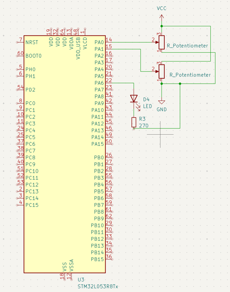
Note: Vcc should be 3.3V.
5. Code:
The entire code as following:
#include  "stm32l0xx.h"

int main(void)
{
	/*Enable clock access to GPIOA*/
	RCC->IOPENR |= RCC_IOPENR_GPIOAEN;

	/*Set PA0 and PA1 as analog Mode*/

	GPIOA->MODER|=GPIO_MODER_MODE0|GPIO_MODER_MODE1;

	/*Set PA6 to alternate function*/

	GPIOA->MODER|=GPIO_MODER_MODE6_1;
	GPIOA->MODER&=~GPIO_MODER_MODE6_0;

	/*Set PA6 AF to AF7*/
	#define AF07	7
	GPIOA->AFR[0]|=(AF07<<GPIO_AFRL_AFSEL6_Pos);


	/*Enable clock access to COMP1 (Same as SYSCFG)*/
	RCC->APB2ENR|=RCC_APB2ENR_SYSCFGEN;

	/*Set the window pin to be PA1*/
	COMP1->CSR&=~ COMP_CSR_COMP1WM;

	/*Set the minus pin to be PA0*/
	COMP1->CSR|=COMP_CSR_COMP1INNSEL_0;
	COMP1->CSR&=~COMP_CSR_COMP1INNSEL_1;

	/*Enable Comparator 1*/
	COMP1->CSR|=COMP_CSR_COMP1EN;


	while(1)
	{
		/*Empty while 1 loop*/
	}

}
6. Results:
When you upload the code, you should get this:
Add Comment