
In the previous guide (here), we took a look at what is parallel port and successfully send byte of data using timer and DMA.
In this guide, we shall add the strobe signal which will be an essential part in the next part of the guide.
In this guide, we shall cover the following:
- What is strobe signal.
- Adding the strobe signal.
- Connecting the LED for strobe indication.
- Results.
1. What is Strobe Signal in Parallel Communication:
Strobe I/O
- In many applications, valid data is present on an external device only at a certain time, so it must be read in at that time.
- E.g. the ASCII-encoded keyboard. When a key is pressed, circuitry on the keyboard sends out the ASCII code for the pressed key on eight parallel data lines, and then sends out a strobe signal on another line to indicate that valid data is present on the eight data lines.
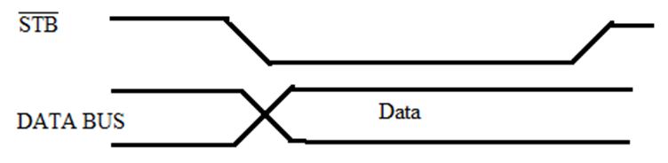
- This timing waveform represents strobe I/O.
- The sending device, such as a keyboard, outputs a parallel data on the data lines, and then outputs an STB signal to let you know that valid data is present.
- For low rates of data transfer, such as from a keyboard to a MP, a simple strobe transfer works well.
- However, for higher speed data transfer, this method does not work because there is no signal which tells the sending device when it is safe to send the next data byte.
- In other words, the sending system might send data bytes faster than the receiving system could read them.
- To prevent this problem, a handshake data transfer scheme is used.
Reference(here).
2. Adding the strobe signal:
Since the strobe signal is active low (detected when signal is low), we could cheat this by using PWM signal with fixed duty cycle to mimic the strobe signal.
Since we already using timer1 to achieve the communication, we can add an extra pin for PWM.
First, we need to find which pins are responsible for TIM1, from the datasheet of STM32F411, we can find this information in table 9: Alternate function mapping.
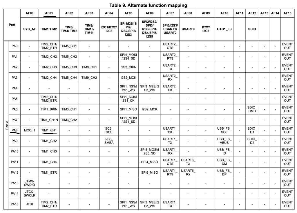
The required pin is PA8 and alternate function 1.
Hence, we start off by enabling clock access to GPIOA as following:
	/*Enable clock access to GPIOA*/
	RCC->AHB1ENR|=RCC_AHB1ENR_GPIOAEN;
Set PA8 as alternate function:
	/*Set PA8 to AF*/
	GPIOA->MODER|=GPIO_MODER_MODE8_1;
	GPIOA->MODER&=~GPIO_MODER_MODE8_0;
Set which alternate function (AF01 in this case):
	/*Set PA8 to AF1*/
	#define AF01		0x01
	GPIOA->AFR[1]|=(AF01<<GPIO_AFRH_AFSEL8_Pos);
In the timer configuration after setting the ARR value, set the CCR1 value to be 100:
TIM1->CCR1=100;
Set channel 1 to be PWM mode 1:
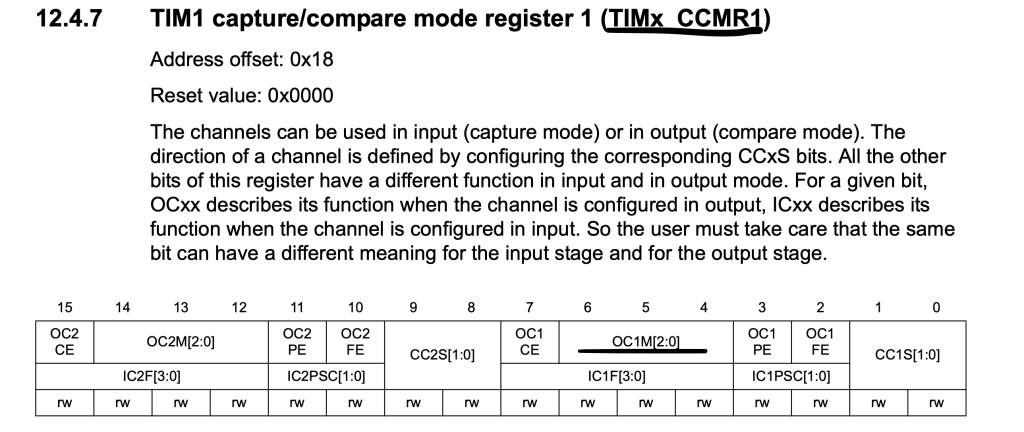
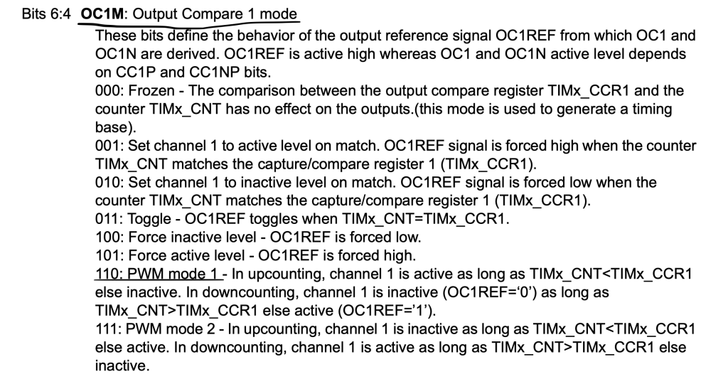
TIM1->CCMR1|=TIM_CCMR1_OC1M_2|TIM_CCMR1_OC1M_1;
Enable Channel1 of the timer:
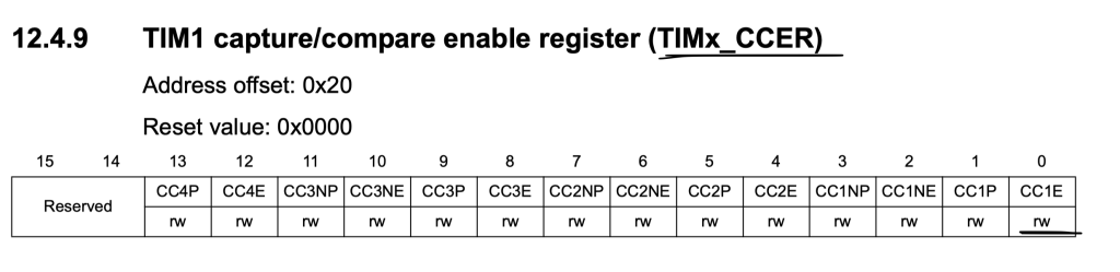
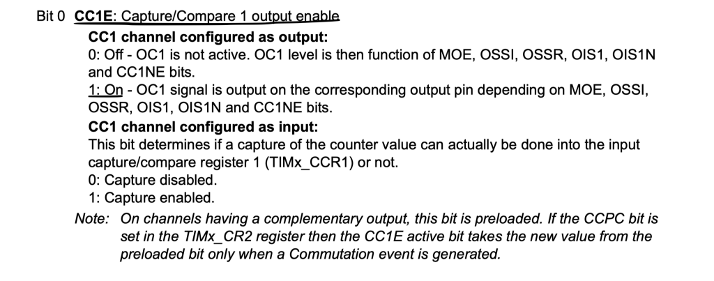
TIM1->CCER|=TIM_CCER_CC1E;
Enable main output as following (only for advanced timers):
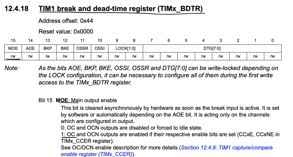
TIM1->BDTR|=TIM_BDTR_MOE;
Hence, the updated code as following:
#include "stm32f4xx.h"
#include "stdint.h"

#include "stdlib.h"

#define data_size 	5
#define CH6 		0x06

uint32_t gpio_pattern[data_size];


#define AF01		0x01


int main(void)
{
	/*GPIO Configuration*/

	/*Enable clock access to GPIOA*/
	RCC->AHB1ENR|=RCC_AHB1ENR_GPIOCEN;

	/*Set PC0 to PC7 as output*/
	GPIOC->MODER|=GPIO_MODER_MODE0_0|GPIO_MODER_MODE1_0|GPIO_MODER_MODE2_0
			|GPIO_MODER_MODE3_0|GPIO_MODER_MODE4_0|GPIO_MODER_MODE5_0|
			GPIO_MODER_MODE6_0|GPIO_MODER_MODE7_0;

	GPIOC->MODER&=~(GPIO_MODER_MODE0_1|GPIO_MODER_MODE1_1|GPIO_MODER_MODE2_1
			|GPIO_MODER_MODE3_1|GPIO_MODER_MODE4_1|GPIO_MODER_MODE5_1
			|GPIO_MODER_MODE6_1|GPIO_MODER_MODE7_1);


	/*PA8 configuration*/

	/*Enable clock access to GPIOA*/
	RCC->AHB1ENR|=RCC_AHB1ENR_GPIOAEN;

	/*Set PA8 to AF*/
	GPIOA->MODER|=GPIO_MODER_MODE8_1;
	GPIOA->MODER&=~GPIO_MODER_MODE8_0;

	/*Set PA8 to AF1*/

	GPIOA->AFR[1]|=(AF01<<GPIO_AFRH_AFSEL8_Pos);


	/*Timer configuration*/

	RCC->APB2ENR  |=  RCC_APB2ENR_TIM1EN;

	TIM1->DIER=TIM_DIER_UDE;

	TIM1->PSC=16000-1; /*16 000 000 / 16 000 =1 000*/
	TIM1->ARR=1000-1; /*1 000 / 1 000 = 10HZ*/

	TIM1->CCR1=100;

	TIM1->CCMR1|=TIM_CCMR1_OC1M_2|TIM_CCMR1_OC1M_1;

	TIM1->CCER|=TIM_CCER_CC1E;

	TIM1->BDTR|=TIM_BDTR_MOE;

	/*DMA configuration*/


	RCC->AHB1ENR|=RCC_AHB1ENR_DMA2EN;

	DMA2_Stream5->CR&=DMA_SxCR_EN;

	while((DMA2_Stream5->CR)&DMA_SxCR_EN){;}

	DMA2_Stream5->CR|=(CH6<<DMA_SxCR_CHSEL_Pos)|DMA_SxCR_MSIZE|DMA_SxCR_PSIZE|
			DMA_SxCR_MINC|DMA_SxCR_CIRC|DMA_SxCR_DIR_0;

	DMA2_Stream5->NDTR=(uint32_t)data_size;

	DMA2_Stream5->PAR=(uint32_t)(&GPIOC->ODR);

	DMA2_Stream5->M0AR=(uint32_t)(gpio_pattern);


	/*Launch DMA*/
	DMA2_Stream5->CR|=DMA_SxCR_EN;

	/*Launch Timer*/
	TIM1->CR1     |= TIM_CR1_CEN;

	srand (TIM1->CNT);

	while(1)
	{
		for (int j=0;j<100000;j++);
		/*Fill the array with random data*/
		for (int i=0; i<data_size;i++)
		{
			gpio_pattern[i]=random()%256;
		}
	}

}
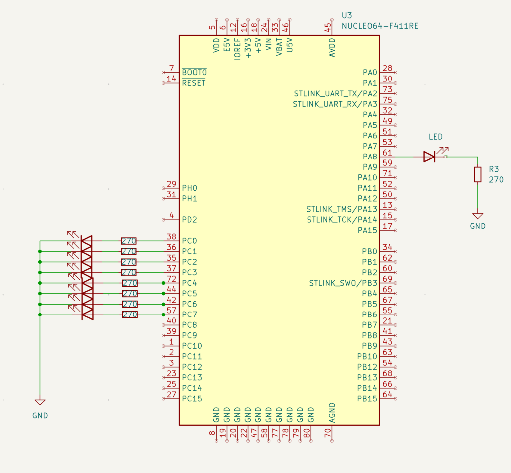
3. Connecting the LED for Strobe Indicator:
For this, you need extra 1 LED and extra 270Ohm Resistor:
4. Results:
Happy coding 🙂
Add Comment