
In this guide, we shall use DMA to toggle LED with a help of a timer to achieve the toggle rate of 1Hz.
In this guide, we shall cover the following :
- GPIO Configuration.
- Timer configuration.
- DMA Configuration.
- Code.
- Results.
1. GPIO Configuration:
Since this guide, the Nucleo-64 F411 is used which has built-in LED which is connected to PA5, hence we shall configure PA5 as output as following:
Enable Clock access to GPIOA:
	/*Enable clock access to GPIOA*/
	RCC->AHB1ENR|=RCC_AHB1ENR_GPIOAEN;
Set pin 5 as output:
	/*Set PA5 as output*/
	GPIOA->MODER|=GPIO_MODER_MODE5_0;
	GPIOA->MODER&=~GPIO_MODER_MODE5_1;
For more details how, please refer to this topic here.
Thats all for GPIO configuration.
Next, timer configuration:
2. Timer configuration:
Since timer1 is used for this operation, we need first to enable clock access to it.
First, we need to find which bus timer1 is connected to.
To find which bus, we need to investigate STM32F411xC/xE block diagram in the datasheet:
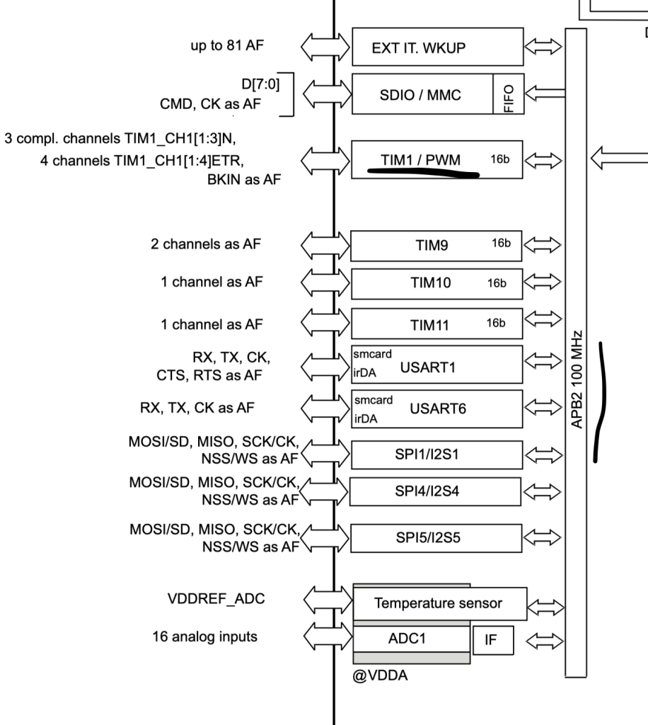
From the block diagram, we can find that TIM1 is connected to APB2 bus. Hence, we can enable clock access to TIM1 as following:
RCC->APB2ENR |= RCC_APB2ENR_TIM1EN;
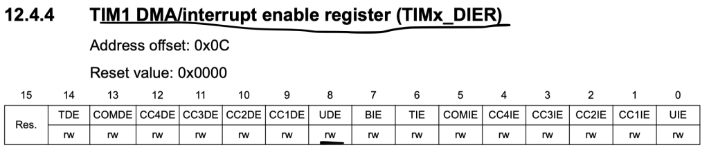
Enable DMA request when update occurs:
Now, set prescaler and ARR to 16000-1 and 1000-1 respectively to achieve 1Hz:
	TIM1->PSC=16000-1; /*16 000 000 / 16 000 =1 000*/
	TIM1->ARR=1000-1; /*1 000 / 1 000 = 1HZ*/
Don’t enable the timer yet.
Now, we shall configure DMA.
3. DMA configuration:
Before configuring the DMA, we need to know which DMA and DMA stream is related to TIM1:
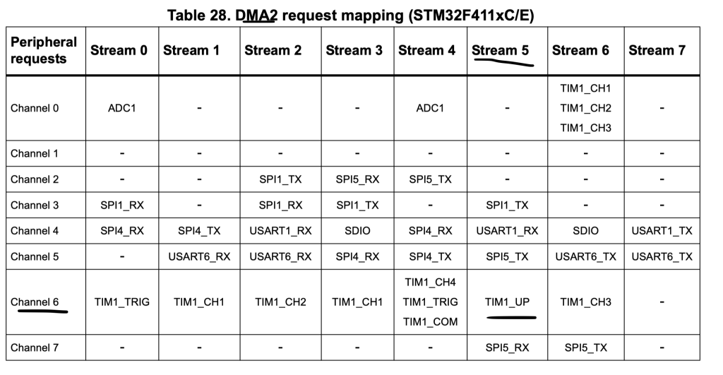
We can find that DMA2 Stream 5 Channel 6 is responsible for TIM1_UP. Hence, we shall enable clock access to DMA2 as following:
RCC->AHB1ENR|=RCC_AHB1ENR_DMA2EN;
Disable the Stream and make sure it is disabled:
	DMA2_Stream5->CR&=DMA_SxCR_EN;
	while((DMA2_Stream5->CR)&DMA_SxCR_EN){;}
Configure the DMA with the following parameters:
- Channel 6.
- Memory and Peripheral size to be word size (32-bit).
- Memory increment mode.
- Circular mode.
- Direction: Memory to peripheral.
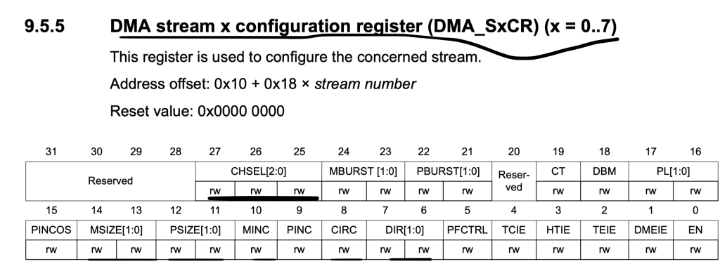
#define CH6 		0x06

	DMA2_Stream5->CR|=(CH6<<DMA_SxCR_CHSEL_Pos)|DMA_SxCR_MSIZE|DMA_SxCR_PSIZE|
			DMA_SxCR_MINC|DMA_SxCR_CIRC|DMA_SxCR_DIR_0;
Set the number of transfers to be data_size (for this guide, it is 2):
DMA2_Stream5->NDTR=(uint32_t)data_size;
Peripheral address to be GPIOA->BSRR register:
DMA2_Stream5->PAR=(uint32_t)(&GPIOA->BSRR);
Set memory address to be the pattern required:
DMA2_Stream5->M0AR=(uint32_t)(gpio_pattern);
The used pattern as following:
#define data_size 	2

uint32_t gpio_pattern[data_size]={GPIO_BSRR_BS5,GPIO_BSRR_BR5};
Enable DMA stream:
	/*Launch DMA*/
	DMA2_Stream5->CR|=DMA_SxCR_EN;
Finally enable the timer:
	/*Launch Timer*/
	TIM1->CR1     |= TIM_CR1_CEN;
4. Code:
The entire code as following:
#include "stm32f4xx.h"
#include "stdint.h"


#define data_size 	2
#define CH6 		0x06

uint32_t gpio_pattern[data_size]={GPIO_BSRR_BS5,GPIO_BSRR_BR5};


int main(void)
{
	/*GPIO Configuration*/

	/*Enable clock access to GPIOA*/
	RCC->AHB1ENR|=RCC_AHB1ENR_GPIOAEN;

	/*Set PA5 as output*/
	GPIOA->MODER|=GPIO_MODER_MODE5_0;
	GPIOA->MODER&=~GPIO_MODER_MODE5_1;

	/*Timer configuration*/

	RCC->APB2ENR  |=  RCC_APB2ENR_TIM1EN;

	TIM1->DIER=TIM_DIER_UDE;

	TIM1->PSC=16000-1; /*16 000 000 / 16 000 =1 000*/
	TIM1->ARR=1000-1; /*1 000 / 1 000 = 1HZ*/


	/*DMA configuration*/


	RCC->AHB1ENR|=RCC_AHB1ENR_DMA2EN;
	DMA2_Stream5->CR&=DMA_SxCR_EN;
	while((DMA2_Stream5->CR)&DMA_SxCR_EN){;}
	DMA2_Stream5->CR|=(CH6<<DMA_SxCR_CHSEL_Pos)|DMA_SxCR_MSIZE|DMA_SxCR_PSIZE|
			DMA_SxCR_MINC|DMA_SxCR_CIRC|DMA_SxCR_DIR_0;

	DMA2_Stream5->NDTR=(uint32_t)data_size;

	DMA2_Stream5->PAR=(uint32_t)(&GPIOA->BSRR);

	DMA2_Stream5->M0AR=(uint32_t)(gpio_pattern);


	/*Launch DMA*/
	DMA2_Stream5->CR|=DMA_SxCR_EN;

	/*Launch Timer*/
	TIM1->CR1     |= TIM_CR1_CEN;

	while(1)
	{

	}


}
5. Results:
Happy coding 🙂
Add Comment