In this guide, we shall discuss what is SPI and how transmit data over SPI.
In this guide, we will cover the following:
- What is SPI.
- SPI pin setup.
- SPI initialize.
- SPI transmite function.
- Result.
1. What is SPI
SPI, which stands for Serial Peripheral Interface, is a standard with a very specific hardware interface. A connection is between a master and a slave, with the master typical being a processor, and the slave being a peripheral such as a sensor, flash memory device, or a modem chip. It can also be used for processor to processor communications, but in this case, an additional handshake signal is often used. There are normally four signals between a master and a slave, the first is a clock signal, and this signal is always driven by the master, regard which device is transmitting. The second line is a data line for data going from the master to the slave, and this is designated as the master output, slave input line, are MOSI for short. It connects the SPI data out connection on the master and to the SPI data in connection on the slave.
The next conductor is for data in the opposite direction and is labelled as the master input slave output line, are MISO for short. The last conductor is slave select with the slave chip selecting input, and is active low.

If you have more than one slave, with the first being perhaps a sensor of some kind, the slave will be dedicated to slave 1. If you add a second sensor, the top 3 interface line will be shared, but it dedicates for slave’s line will be required for the second device, and the same is true of course for each of additional slave device.

Most processors have a maxim of 4 slave selected lines. The four lines could be used effectively as a multiplexed address lines to access more than 4 slaves. You cannot have more than one master on the bus, since the interface is not support coordination between two masters as to which one is controlling the bus.
Transmissions are typically sent as a sequence of bytes, but without a formal protocol, there is nothing restricting communication being byte based. Typical by frame sizes, are in 8 to 32 bits range. Also note the bytes and packets are not acknowledged as they are in i2c, and you could have a master synching communicating with the slave but, you don’t really know of your communications are being received OK. However, some slave devices will echo bytes sent to it, which provides an acknowledgement to the master. it is how the data lines are synchronized with a clock signal.
Clock Polarity and Phasing
There are four different modes available, one mode each combination clocking in a low state and high state, with a data being read in a rising edge or falling edge of the clock signal. For modes 0 and 1, the clock is low in idle, which is referred to as clock and 0, For modes 2 and 3 then the clock is in high state when idle, so it has polarity , one , For modes 0 and 2, the data will be sampled by the receiving device on the leading edge of a clock signal. Relative to the idle state, which is referred to a clock phase of zero. So for mode 0, this means the rising edge of the clock and for mode 2, means the following edge of the clock, the other two modes, use a clock phase 1 which means that trailing edge of clock as a returns to an idle state. And this translates to a following edge for mode 1 and the rising edge for mode 3. Mode 0 is the most commonly supported setting. If multiple slaves in the same bus, you may have to reconfigure the settings for the master to which modes when you want to communicate with a different slave.

2. SPI pins Setup:
First, we need to find which pins are related to SPI. This can be found in SPI1 alternate function remapping section of the reference manual.
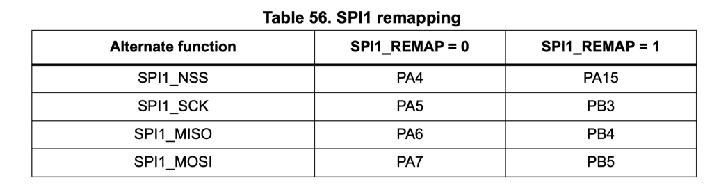
Since we shall use software slave management, we shall not use NSS pin. Hence, the pins required are:
- PA5 for SCK
- PA6 for MISO
- PA7 for MOSI
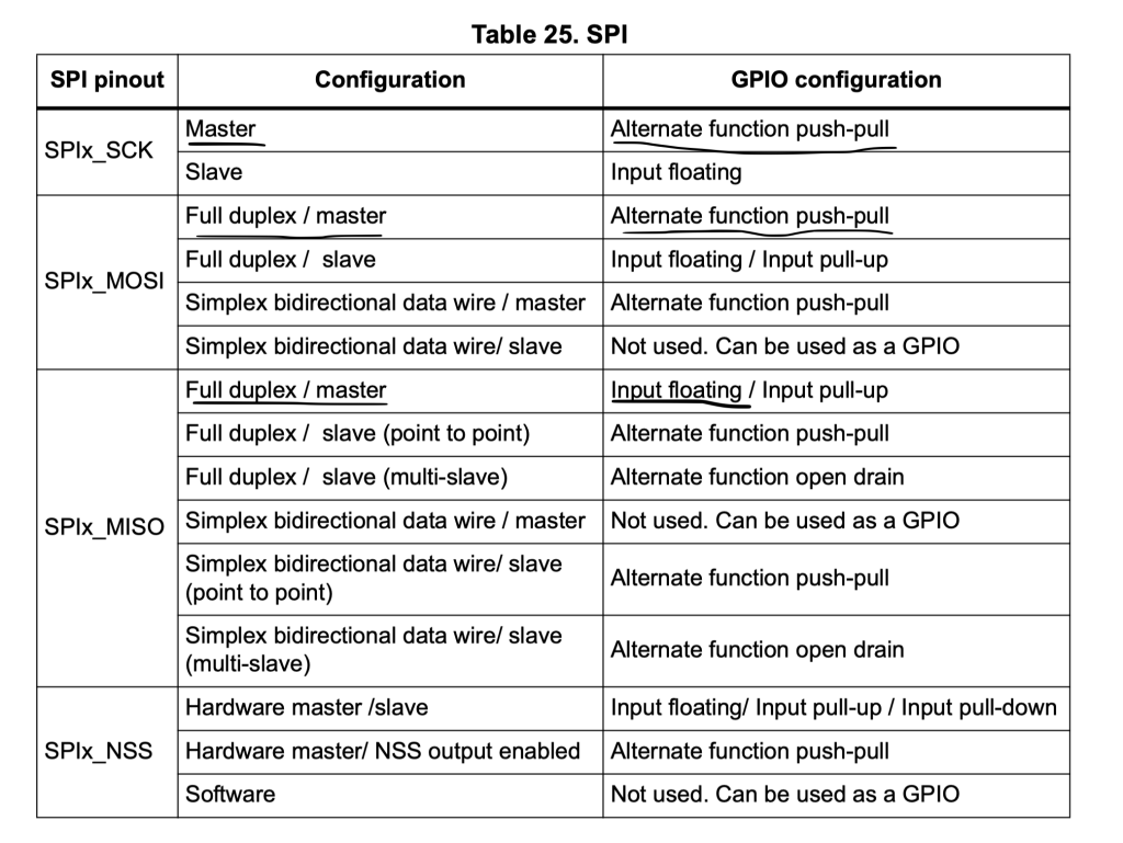
The pins configuration as following:
Hence, create a new source and header file with name of spi.c and spi.h respectively.
Within the header file, include the following:
#include "stdint.h"
Declare the following functions:
void spi_init(void);
void spi_transmit(uint8_t *data,uint32_t size);
void cs_low();
void cs_high();
Hence, the header file as following:
#ifndef SPI_H_
#define SPI_H_

#include "stdint.h"


void spi_init(void);
void spi_transmit(uint8_t *data,uint32_t size);
void cs_low();
void cs_high();


#endif /* SPI_H_ */
Within the source file, we start with spi_init function:
void spi_init(){within the function, we shall configure both SPI and GPIO.
For the GPIO:
	//Enable Port A clock
	RCC->APB2ENR |= RCC_APB2ENR_IOPAEN;
	RCC->APB2ENR |= RCC_APB2ENR_AFIOEN;
	/* PA5-SCK and PA7-MOSI */
	//Mode: Output, Speed: 10MHz
	GPIOA->CRL &= ~(GPIO_CRL_MODE5);
	GPIOA->CRL &= ~(GPIO_CRL_MODE7);
	GPIOA->CRL |= (GPIO_CRL_MODE5_0);
	GPIOA->CRL |= (GPIO_CRL_MODE7_0);
	//Alternate function push-pull
	GPIOA->CRL &= ~(GPIO_CRL_CNF5);
	GPIOA->CRL &= ~(GPIO_CRL_CNF7);
	GPIOA->CRL |= (GPIO_CRL_CNF5_1);
	GPIOA->CRL |= (GPIO_CRL_CNF7_1);

	/* PA5-MISO */
	//Mode input
	GPIOA->CRL &= ~(GPIO_CRL_MODE6);
	//Floating input
	GPIOA->CRL &= ~(GPIO_CRL_CNF6);
	GPIOA->CRL |= (GPIO_CRL_CNF6_0);

	//Remap 0: PA5, PA6, PA7
	AFIO->MAPR &= ~(1UL << 0);

	/*Configure PA0 as output CS*/
	GPIOA->CRL|=GPIO_CRL_MODE0;
	GPIOA->CRL&=~(GPIO_CRL_CNF0);
Thats all for the GPIO.
3. SPI initializing:
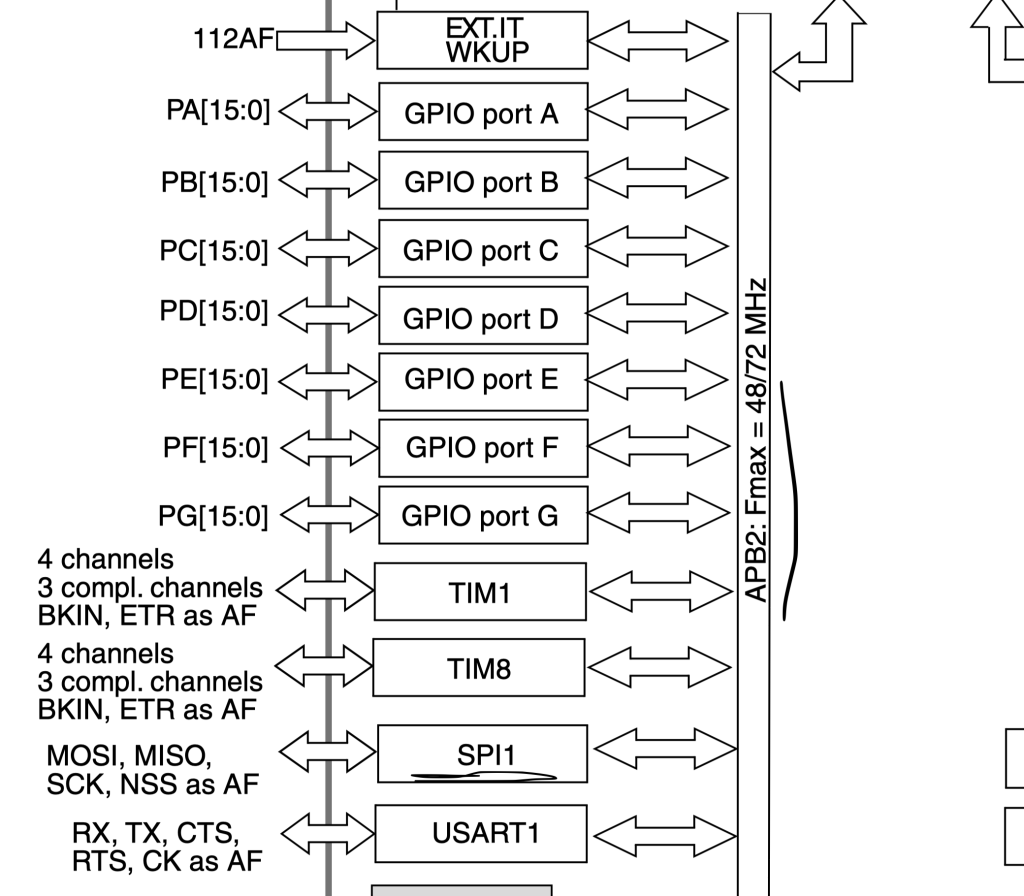
Before we start with the initializing the SPI, we need to enable clock access to SPI. From the datasheet, from the block diagram, we can find the SPI1 is connected to APB2 BUS:
	//Enable SPI Clock
	RCC->APB2ENR |= RCC_APB2ENR_SPI1EN;
Then we set the SPI
- Set SSM and SSI
Set SPI to master mode - Finally enable SPI module
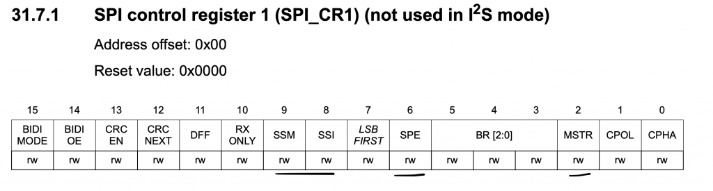
	//Mode: Master
	SPI1->CR1 |= SPI_CR1_MSTR;
	//Baud rate to (8MHz / 2 = 4MHz)
	SPI1->CR1 &= ~SPI_CR1_BR;
	//MSB first
	SPI1->CR1 &= ~(SPI_CR1_LSBFIRST);
	//Full duplex (Transmit/Receive)
	SPI1->CR1 &= ~(SPI_CR1_RXONLY);
	//Data format 8-bit
	SPI1->CR1 &= ~(SPI_CR1_DFF);
	//Software Slave select
	SPI1->CR1 |= SPI_CR1_SSI;
	SPI1->CR1 |= SPI_CR1_SSM;
	//SPI Enable
	SPI1->CR1 |= SPI_CR1_SPE;
	//Clear initial flags
	(void)SPI1->SR;
4. SPI transfer function:
We start off by declaring the following function:
void spi_transmit(uint8_t *data,uint32_t size)
The function takes the following two parameters:
- pointer to array that holds the data to be transmitted.
- Length of the data.
Within the function, declare the following variable:
uint32_t i=0;
Then:
	while(i<size)
	{
		 /*Wait for the TXE bit to set in the Status Register*/
		/*This will indicate that the transmit buffer is empty*/
		 while (!((SPI1->SR)&(1<<1))) {};
		   /*Write the data to the Data Register*/
		   SPI1->DR = data[i];
		   i++;
	}
We shall transmit the data one after the other as following:
While the i is less than the size of the data, do the following:
- Wait until TXE bit is set (indicates that TX buffer is empty).
- Send the data by writing it to DR register.
- increment the counter.
- Do this until i is equal or bigger than size.
Outside the while loop:
 /*Wait for the TXE bit to set in the Status Register*/
	 while (!((SPI1->SR)&(1<<1))) {};

	 /*Wait for the BSY bit to reset in the Status Register*/
	 while (((SPI1->SR)&(1<<7))) {};

	 /*Clear OVR flag*/
	(void) SPI1->DR;
	(void) SPI1->SR;
For chip select:
void cs_low()
{
	GPIOA->BSRR=GPIO_BSRR_BR0;
}

void cs_high()
{
	GPIOA->BSRR=GPIO_BSRR_BS0;
}
Hence, the entire source code as following:
/*
 * spi.c
 *
 *  Created on: Mar 1, 2023
 *      Author: hussamaldean
 */


#include "spi.h"
#include "stm32f1xx.h"


void spi_init(void)
{
	//Enable Port A clock
	RCC->APB2ENR |= RCC_APB2ENR_IOPAEN;
	RCC->APB2ENR |= RCC_APB2ENR_AFIOEN;
	/* PA5-SCK and PA7-MOSI */
	//Mode: Output, Speed: 10MHz
	GPIOA->CRL &= ~(GPIO_CRL_MODE5);
	GPIOA->CRL &= ~(GPIO_CRL_MODE7);
	GPIOA->CRL |= (GPIO_CRL_MODE5_0);
	GPIOA->CRL |= (GPIO_CRL_MODE7_0);
	//Alternate function push-pull
	GPIOA->CRL &= ~(GPIO_CRL_CNF5);
	GPIOA->CRL &= ~(GPIO_CRL_CNF7);
	GPIOA->CRL |= (GPIO_CRL_CNF5_1);
	GPIOA->CRL |= (GPIO_CRL_CNF7_1);

	/* PA5-MISO */
	//Mode input
	GPIOA->CRL &= ~(GPIO_CRL_MODE6);
	//Floating input
	GPIOA->CRL &= ~(GPIO_CRL_CNF6);
	GPIOA->CRL |= (GPIO_CRL_CNF6_0);

	//Remap 0: PA5, PA6, PA7
	AFIO->MAPR &= ~(1UL << 0);

	/*Configure PA0 as output CS*/
	GPIOA->CRL|=GPIO_CRL_MODE0;
	GPIOA->CRL&=~(GPIO_CRL_CNF0);


	//Enable SPI Clock
	RCC->APB2ENR |= RCC_APB2ENR_SPI1EN;

	//Mode: Master
	SPI1->CR1 |= SPI_CR1_MSTR;
	//Baud rate to (8MHz / 2 = 4MHz)
	SPI1->CR1 &= ~SPI_CR1_BR;
	//MSB first
	SPI1->CR1 &= ~(SPI_CR1_LSBFIRST);
	//Full duplex (Transmit/Receive)
	SPI1->CR1 &= ~(SPI_CR1_RXONLY);
	//Data format 8-bit
	SPI1->CR1 &= ~(SPI_CR1_DFF);
	//Software Slave select
	SPI1->CR1 |= SPI_CR1_SSI;
	SPI1->CR1 |= SPI_CR1_SSM;
	//SPI Enable
	SPI1->CR1 |= SPI_CR1_SPE;
	//Clear initial flags
	(void)SPI1->SR;


}

void spi_transmit(uint8_t *data,uint32_t size)
{
	uint32_t i=0;

	while(i<size)
	{
		 /*Wait for the TXE bit to set in the Status Register*/
		/*This will indicate that the transmit buffer is empty*/
		 while (!((SPI1->SR)&(1<<1))) {};
		   /*Write the data to the Data Register*/
		   SPI1->DR = data[i];
		   i++;
	}
	 /*Wait for the TXE bit to set in the Status Register*/
	 while (!((SPI1->SR)&(1<<1))) {};

	 /*Wait for the BSY bit to reset in the Status Register*/
	 while (((SPI1->SR)&(1<<7))) {};

	 /*Clear OVR flag*/
	(void) SPI1->DR;
	(void) SPI1->SR;
}


void cs_low()
{
	GPIOA->BSRR=GPIO_BSRR_BR0;
}

void cs_high()
{
	GPIOA->BSRR=GPIO_BSRR_BS0;
}
Within main.c:
#include "spi.h"

uint8_t data[5]={0x01,0x02,0x03,0x04,0x05};


int main(void)
{
	spi_init();

	while(1)
	{	cs_low();
		spi_transmit(data, 5);
		cs_high();
		for (int i=0;i<10000;i++);
	}
}
5. Code:
You may download the source code from here:
6. Results:
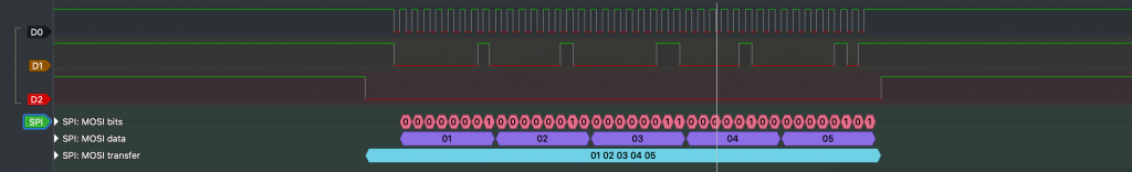
When you connect logic analyzer to PA5, PA7 and PA0, you will get the following results:
Happy coding 🙂
Add Comment