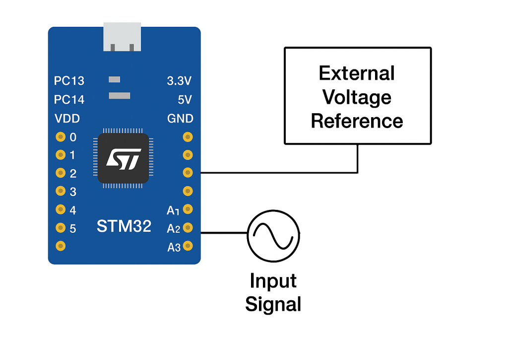
Using an external voltage reference can significantly improve the accuracy and stability of ADC measurements on the STM32F4. By providing a precise and low-noise reference voltage, the ADC can achieve more consistent conversion results, especially in applications sensitive to power-supply variations.
In this guide, we shall cover the following:
- Importance of external voltage reference.
- Hardware modification.
- STM32CubeIDE setup.
- Firmware development.
- Results.
1. Importance of External Voltage Reference:
A stable and accurate reference voltage is one of the most critical elements in achieving high-quality analog-to-digital conversions on the STM32F4 series. The ADC converts an analog input into a digital value by comparing the input voltage against a reference voltage—so any noise, drift, or instability in this reference directly and proportionally affects every ADC reading. When relying on the internal reference (often tied to the MCU’s supply rail or internal buffer), variations in load, temperature, and power integrity can introduce significant measurement errors that cannot be eliminated through software filtering alone. Using an external precision reference voltage provides a clean, low-noise, and temperature-stable reference, ensuring that the ADC’s full resolution is genuinely usable and not degraded by fluctuations in the supply.
An external voltage reference is especially important when the ADC must measure low-level signals, monitor sensors requiring tight accuracy, or operate in electrically noisy environments. Many real-time control systems, such as motor drives, instrumentation amplifiers, battery monitors, and medical devices, demand repeatable and predictable readings where even millivolts matter. External references are designed to maintain ultra-low drift over temperature, superior line and load regulation, and extremely low noise performance—qualities that significantly improve the ADC’s effective number of bits (ENOB). Even if the STM32F4 ADC is natively 12-bit, a poor reference voltage can reduce the usable resolution to 8 or 9 bits, wasting system capability.
Additionally, external references allow designers to choose a reference voltage tailored to the application. A 2.5V, 3.0V, or 1.8V reference may be preferred depending on sensor output range, desired dynamic range, or system power architecture. A higher precision reference expands the signal-to-noise ratio and enables more reliable calibration, especially in long-running or safety-critical systems. Since the ADC’s digital output is always scaled relative to Vref+, any improvement in the reference voltage directly enhances absolute accuracy, linearity, gain error, and long-term stability. In summary, an external voltage reference transforms the ADC from a general-purpose converter into a precision measurement instrument by removing power-domain interference, guaranteeing stable comparisons, and unlocking the true resolution capability of the STM32F4 ADC.
2. Hardware Modification:
In this guide, I shall use STM32F407 Black which is shown in the picture below:

From the schematic of the board, we can see that R11 (0R) is connected between 3V3 and Vref+, we need to remove the resistor to supply our own voltage for the external voltage reference.
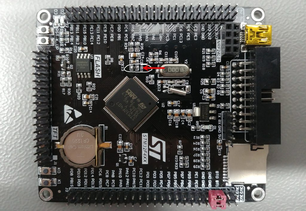
Note: The location might be different from the one in the picture. It depends on the hardware revision.
3. STM32CubeIDE Setup:
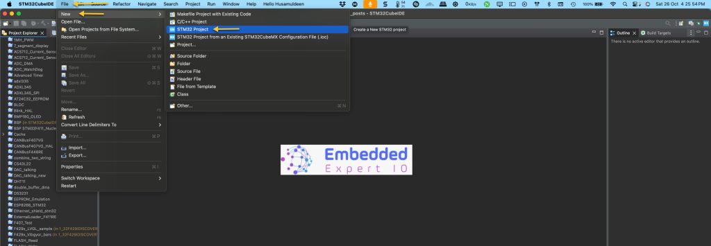
Open STM32CubeIDE after selecting the workspace and create new project as following:
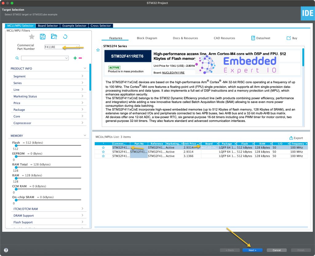
Select the MCU (Ensure that you are selecting a one with oversampling like STM32L476RG):
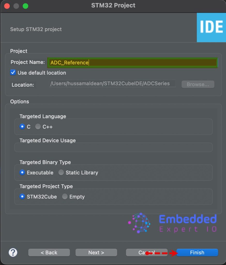
Give the project a name:
Once the project has been created, STM32CubeMX tab will appear.
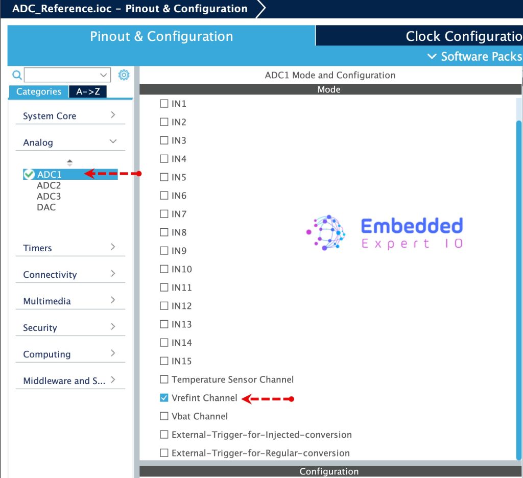
From analog, First, enable Vrefint channel as follows:
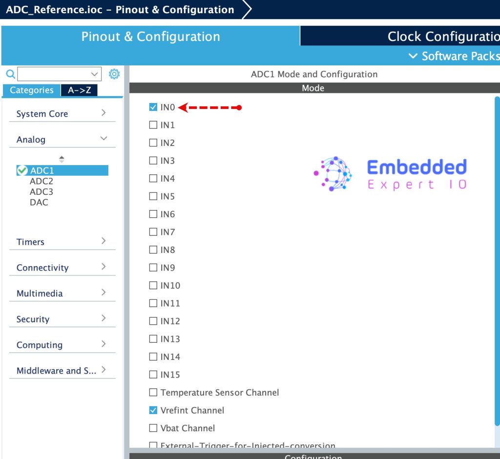
Next, enable IN0 for the ADC as follows:
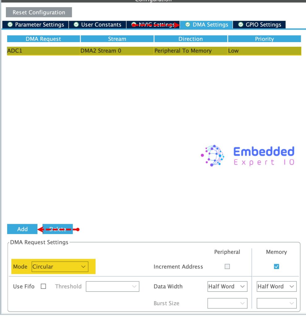
Next, configure the DMA as follows:
- Mode to Circular.
- Data Width to half word for both.
- Memory increment mode.
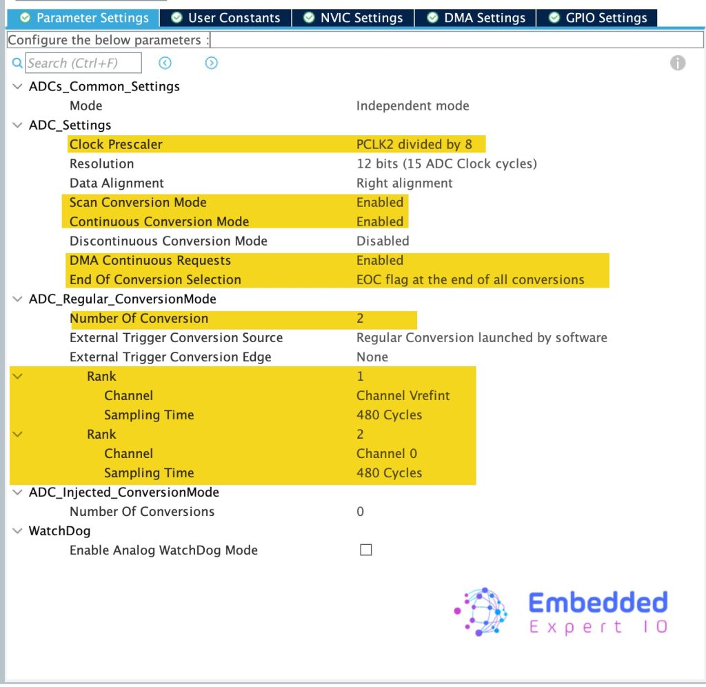
Next, configure the ADC as follows:
- Set Clock Prescaler to PCLK/8.
- Number of Conversion to 2.
- Scan Mode will be enabled once you set the number of conversion.
- DMA Continuous Mode to enabled.
- Rank 1, set it to Channel Vrefint and sampling time to 480 cycles.
- Rank 2, set it to Channel 0 and sampling time to 480 cycles.
Thats all for the STM32CubeIDE setup.
Save the project and this will generate the code.
4. Firmware Development:
Once the project has been generated, main.c will be opened.
Within the main.c, in user code begin PV, declare an array to hold the ADC measurement values as follows:
uint16_t ADC_VAL[2];
Next, declare two variables to hold the voltage of Vref and IN0 as follows:
int voltage;
int vref = 0;
Next, we shall get the address of the reference calibration value as follows:
#define Vref_CAL *VREFINT_CAL_ADDR
This can be found in the datasheet of the STM32 as follows:
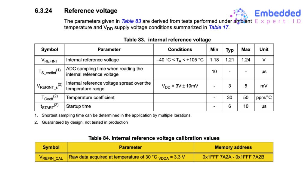
ST in their header file, already provided the address as follows:
#define VREFINT_CAL_ADDR ((uint16_t*) (0x1FFF7A2AU)) /* Internal voltage reference, address of parameter VREFINT_CAL: VrefInt ADC raw data acquired at temperature 30 DegC (tolerance: +-5 DegC), Vref+ = 3.3 V (tolerance: +-10 mV). */
Next, in user code begin 0, declare the adc conversion completed callback:
void HAL_ADC_ConvCpltCallback(ADC_HandleTypeDef *hadc)
{
	vref = 3300*Vref_CAL/ADC_VAL[0];
}
In use code begin 2 in the main function, start the ADC in DMA mode as follows:
HAL_ADC_Start_DMA(&hadc1, ADC_VAL, 2);
Thats all for the firmware development.
Build the project and run it.

5. Results:
When Vref is 3.00V:
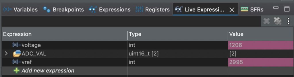
Vref measured 2995 mV.
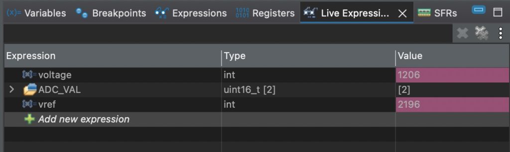
Vref is 2.2
Vref is 1.6
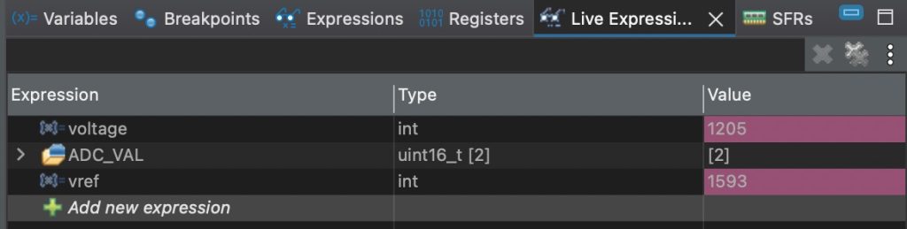
The results are what is expected. The slight difference is due to accuracy of the power supply.
Happy coding 😉
Add Comment