In the previous guide (here), we saw to configure the ADXL345 to work in I2C mode and get the acceleration values.
In this guide, we shall use the same sensor is SPI mode.
In this guide, we shall cover the following:
- Connection.
- Pin configuration.
- SPI configuration.
- SPI write function.
- SPI read function.
- Slave select function.
- Slave deselect function.
1. Connection:
The connection between STM32F411-Nucleo and adxl345 module is as following:
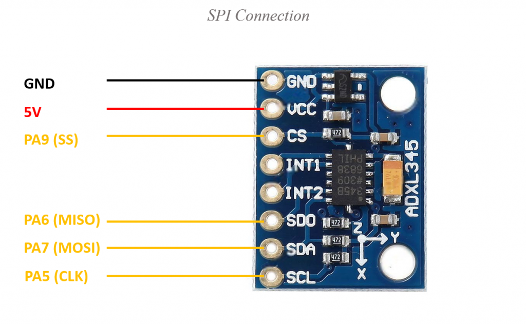
| STM32F4 | ADXL345 |
| 5V | Vcc |
| GND | GND |
| PA9 | CS |
| PA6 | SDO |
| PA7 | SDA |
| PA5 | SCL |
2. Pins Configuration:
Since the required pins are PA5 to PA7 and PA9. Hence, we start of by enabling clock access to GPIOA:
RCC->AHB1ENR|=RCC_AHB1ENR_GPIOAEN; //enable clock for GPIOA
Set PA5,PA6 and PA7 to alternate function:
GPIOA->MODER|=GPIO_MODER_MODE5_1|GPIO_MODER_MODE6_1|GPIO_MODER_MODE7_1; //set PA5, PA6 and PA7 to alternate function mode
GPIOA->MODER &=~(GPIO_MODER_MODE5_0|GPIO_MODER_MODE6_0|GPIO_MODER_MODE7_0);
Set PA9 to General purpose output:
GPIOA->MODER|=GPIO_MODER_MODE9_0;
GPIOA->MODER&=~(GPIO_MODER_MODE9_1);
Since SPI is AF05, we need to set PA5, PA6 and PA7 to AF5 in AFRL register:
GPIOA->AFR[0]|=(0x05<<20)|(0x05<<24)|(0x05<<28);
3. SPI Configuration:
In order to make ADXL345 working in SPI, the SPI parameters shall be as following:
- SPI clock shall not be greater than 4MHz (Clock divider of 4 in this guide (F4 default frequency is 16MHz)).
- CPOL=1 and CPHA=1.
- MSB first.
- Master mode.
For more information about SPI, please check this guide here.
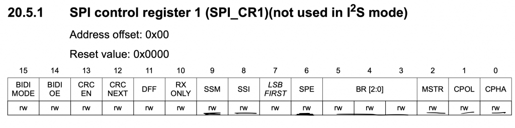
Hence, the configuration as following:
/*Enable clock access to SPI1 module*/
	RCC->APB2ENR |= RCC_APB2ENR_SPI1EN;

	/*Set clock to fPCLK/4*/
	SPI1->CR1 |=(1U<<3);
	SPI1->CR1 &=~(1U<<4);
	SPI1->CR1 &=~(1U<<5);

	/*Set CPOL to 1 and CPHA to 1*/
	SPI1->CR1 |=(1U<<0);
	SPI1->CR1 |=(1U<<1);

	/*Enable full duplex*/
	SPI1->CR1 &=~(1U<<10);

	/*Set MSB first*/
	SPI1->CR1 &= ~(1U<<7);

	/*Set mode to MASTER*/
	SPI1->CR1 |= (1U<<2);

	/*Set 8 bit data mode*/
	SPI1->CR1 &= ~(1U<<11);

	/*Select software slave management by
	 * setting SSM=1 and SSI=1*/
	SPI1->CR1 |= (1<<8);
	SPI1->CR1 |= (1<<9);

	/*Enable SPI module*/
	SPI1->CR1 |= (1<<6);
4. SPI Write function:
void spi1_transmit(uint8_t *data,uint32_t size)
{
	uint32_t i=0;

	while(i<size)
	{
		/*Wait until TXE is set*/
		while(!(SPI1->SR & (SPI_SR_TXE))){}

		/*Write the data to the data register*/
		SPI1->DR = data[i];
		i++;
	}
	/*Wait until TXE is set*/
	while(!(SPI1->SR & (SPI_SR_TXE))){}

	/*Wait for BUSY flag to reset*/
	while((SPI1->SR & (SPI_SR_BSY))){}

	/*Clear OVR flag*/
	(void)SPI1->DR;
	(void)SPI1->SR;
}
5. SPI Read function:
void spi1_receive(uint8_t *data,uint32_t size)
{
	while(size)
	{
		/*Send dummy data*/
		SPI1->DR =0;

		/*Wait for RXNE flag to be set*/
		while(!(SPI1->SR & (SPI_SR_RXNE))){}

		/*Read data from data register*/
		*data++ = (SPI1->DR);
		size--;
	}
}
6. Slave Select:
In order to select the slave, you need to set CS line to 0 for the specific slave.
GPIOA->BSRR=GPIO_BSRR_BR9;
7. Slave Deselect:
To deselect the salve, set the pin to high.
GPIOA->BSRR=GPIO_BSRR_BS9;
In part 2, we shall see how to read the adxl345 data.
Stay tuned and happy coding 🙂
Add Comment