

In the previous guide (here), we took a look at the advanced control timer and how to generate PWM signal with complementary output. In this guide, we shall introduce the dead-time between each main channel and it’s complementary.
In this guide, we shall cover the following:
- What is dead time.
- Dead time calculation.
- Adding the dead time.
- Results.
1. What is Dead Time:
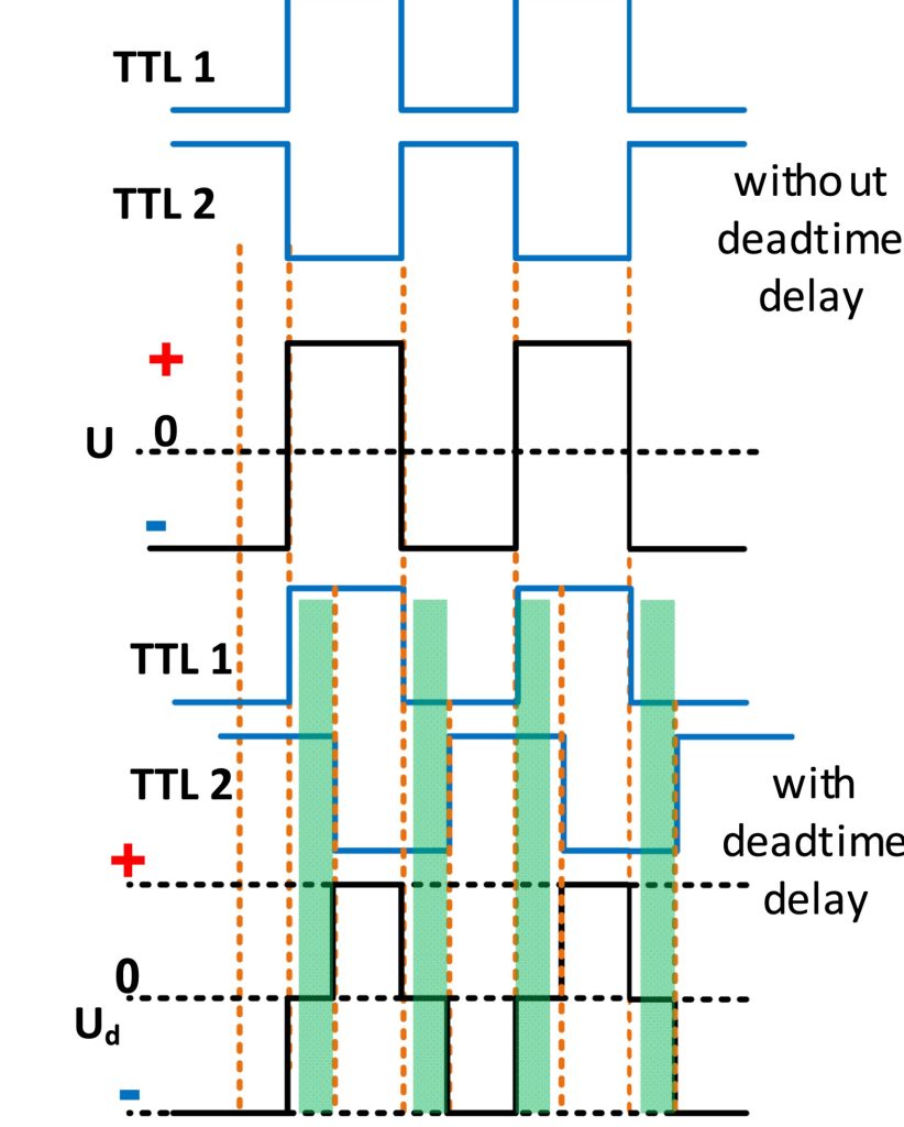
Deadtime (it is the time delay between the gating signals of switching devices to prevent them from turn-on or turn-off at the same time and therefore to avoid short circuits) is a critical parameter for PWM voltage generating devices to power electronic devices and varies from nanosecond to several microseconds.
2. Dead Time Calculation:
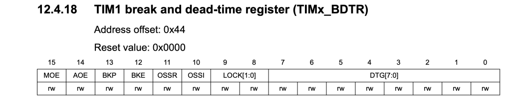
Since the value of the dead time generator is 8-bit length DTG[7:0] as shown below:
The calculation as following:
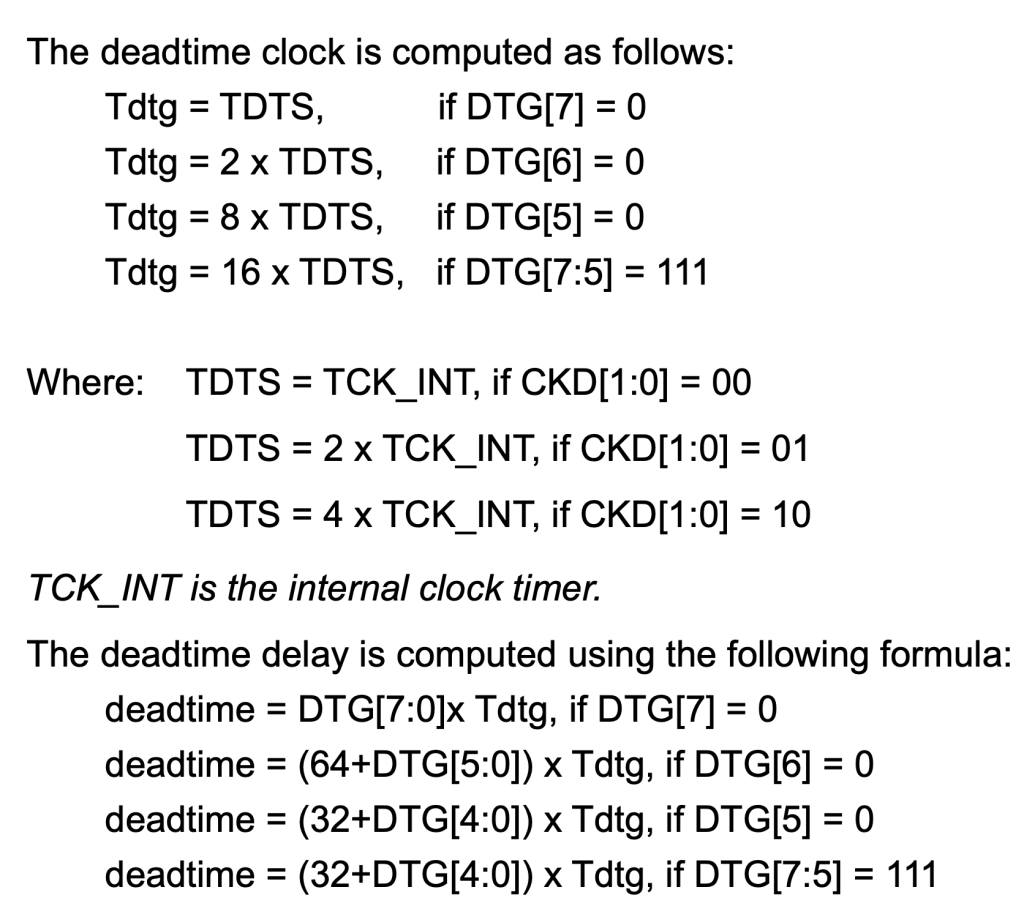
Example of the calculation:

Related course
Put dead time in context
A gap between switching edges has a practical purpose in a motor drive. Explore the course’s treatment of inductive energy, shoot-through and dead time alongside motor-control fundamentals. The hands-on sequence uses its own brushed DC platform, so hardware details differ here.
3. Adding the Dead Time:
From the previous guide, before enabling the MOE (Main Output Enable), we can add the dead time as following:
	/*Set the dead timer*/

	TIM1->BDTR|=(0xFF<<TIM_BDTR_DTG_Pos);
Hence, the updated code as following:
#include "stm32f4xx.h"

/*
 * PA7->TIM1_CH1N
 * PA8->TIM1_CH1
 * */

#define TIM1AF	0x01


int main(void)
{
	/*Enable clock access to GPIOA*/
	RCC->AHB1ENR|=RCC_AHB1ENR_GPIOAEN;

	/*Configure PA7 and PA8 as alternate mode*/
	GPIOA->MODER|=(GPIO_MODER_MODE7_1)|(GPIO_MODER_MODE8_1);
	GPIOA->MODER&=~(GPIO_MODER_MODE7_0)|(GPIO_MODER_MODE8_0);

	/*Select which alternate function*/
	/*Set PA7 to AF01*/
	GPIOA->AFR[0]|=(TIM1AF<<GPIO_AFRL_AFSEL7_Pos);
	/*Set PA8 to AF01*/
	GPIOA->AFR[1]|=(TIM1AF<<GPIO_AFRH_AFSEL8_Pos);

	/*Timer configuration*/

	/*Enable clock access to TIM1*/
	RCC->APB2ENR|=RCC_APB2ENR_TIM1EN;

	/*Set Prescaler to 16-1 to get 1MHz*/
	TIM1->PSC=15;

	/*Set ARR to 1000 to get 1KHz*/

	TIM1->ARR=1000;

	/*Configure CH1 to be PWM channel*/

	TIM1->CCMR1|=TIM_CCMR1_OC1M_2|TIM_CCMR1_OC1M_1;

	/*Enable CH1 and CH1 complementary output*/

	TIM1->CCER|=TIM_CCER_CC1E|TIM_CCER_CC1NE;


	/*Set the dead timer*/

	TIM1->BDTR|=(0xFF<<TIM_BDTR_DTG_Pos);

	/*Enable Main output*/

	TIM1->BDTR|=TIM_BDTR_MOE;

	/*Set Duty cycle to be 500 (50%)*/
	TIM1->CCR1=500;

	/*Enable TIM1*/

	TIM1->CR1|=TIM_CR1_CEN;


	while(1)
	{

	}

}
4. Results:
By using oscilloscope and probing both PA7 and PA8, we shall get the following:
The cursor measures a dead time of 62uS which is near the calculated value of 63uS.
With this, you have successfully generated deadtime for two PWM signal and can be implemented in ton of applications.
Happy coding 🙂
thank you very much
its very usefull
whould you pls talk about dead time insertion on pwm
thanks
This is how to add dead time for pwm signal.