

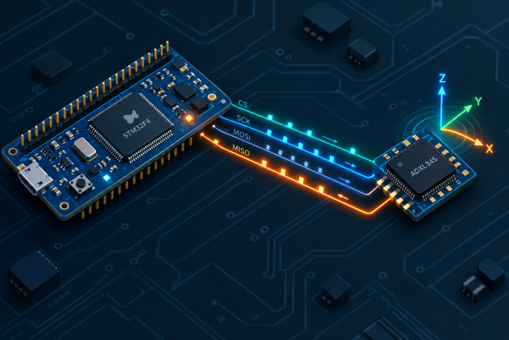
Unlike UART or I2C, an SPI master never simply listens: clocks only run while the master transmits, so every read is inherently a simultaneous write of dummy bytes whose only purpose is to keep SCK toggling. In this part we implement a polling-mode receive function, deal with the subtle consequences of full-duplex operation — stale RXNE flags and overrun errors left behind by transmit-only code — and learn why releasing chip select at exactly the right moment matters just as much here as it did for transmission.
In this guide, we shall cover the following:
- Introduction.
- Firmware Development.
- Results.
1. Introduction:
In the previous part we built a function that pushes bytes out over SPI, and if transmission felt natural, that is because it matches our mental model of “sending data”. Reception is where SPI stops behaving like the interfaces you already know. An I²C master can issue a read and simply wait for the slave to talk; a UART receiver listens whenever data arrives. An SPI master can do neither, because the bus has no life of its own: SCLK only toggles while the master itself is transmitting, so the only way to move the slave’s data is to keep clocking out bytes of our own.
Every SPI transfer is therefore an exchange. While our bits travel along MOSI into the slave, the slave’s bits travel back along MISO, both moved by the very same clock edges. To receive N bytes, we must transmit N bytes — dummy bytes, whose contents the slave ignores — and collect whatever comes back. Reception on a master is a write and a read happening simultaneously, and the code must juggle both directions at once: TXE tells us when to feed in the next dummy byte, RXNE tells us when the reply has landed in the data register.
This full-duplex machinery has a consequence that bites nearly everyone the first time: transmit-only code still receives. Every byte we sent in the previous part was also received by our own SPI peripheral, and since we never read DR, that data piles up behind a stale RXNE flag and an overrun error. A receive function that does not clean up this state will hand you one garbage byte on its first call and a set OVR flag as a bonus — clearing it on the F4 requires the documented read-DR-then-read-SR sequence from RM0090, so we will handle it explicitly.
Chip select, meanwhile, acquires real meaning. For an actual slave, CS is not an electrical formality but part of the protocol: many devices interpret a rising edge on CS as “transaction over” and reset their interface logic. A multi-byte read that is split across two CS assertions will return garbage, so all the reads in this part will take place under a single, carefully timed CS pulse — with the BSY wait from the previous part still guarding the very last bit.
A real device: the ADXL345
All of this is easiest to absorb with a real slave on the bench instead of a theoretical one, so for the rest of this guide we will use the ADXL345 three-axis accelerometer from Analog Devices as the sensor we read from and write to. It is cheap, widely available, forgiving of beginner mistakes, and — more importantly — it is an excellent stand-in for an entire class of devices: gyroscopes, magnetometers, pressure sensors, and flash memories all talk in fundamentally the same register-based way.
On its own, the ADXL345 measures acceleration on three axes with selectable full-scale ranges from ±2 g to ±16 g, up to 13-bit resolution, output data rates from 0.1 Hz to 3200 Hz, plus a 32-sample FIFO and built-in activity, tap, and free-fall detection. We will only need a small corner of that feature set: identify the chip, configure it, and stream X/Y/Z samples.
| Parameter | ADXL345 requirement |
|---|---|
| Logic level | 2.0–3.6 V — directly compatible with 3.3 V STM32 GPIO |
| Bus | 4-wire SPI (3-wire mode optional), I²C also available |
| SPI modes | 0 and 3 |
| Frame format | 8-bit, MSB first |
| Maximum SCLK | 5 MHz |
That last row deserves attention before we write any code, because it changes our CubeMX settings. On a 168 MHz STM32F407, SPI1 hangs off the 84 MHz APB2 bus, and the nearest prescaler, /16, yields 5.25 MHz — a hair above the sensor’s limit and therefore out of spec. The correct choice is /32, giving a comfortably legal 2.625 MHz (on SPI2/SPI3, fed from the 42 MHz APB1 clock, the equivalent safe choice is /16). The lesson generalizes to every project you will ever build: the SPI clock is chosen from the slave’s datasheet, never from a preference for speed.
The register protocol
The ADXL345 is organized as a register map spanning addresses 0x00–0x39, and every transaction opens with a single command byte that tells the slave what we intend to do:
| Bit(s) | Field | Meaning |
|---|---|---|
| 7 | R/W | 1 = read, 0 = write |
| 6 | MB | 1 = multibyte transfer, address auto-increments |
| 5:0 | A5:A0 | 6-bit register address |
Writing to the sensor is pure transmission — the exact function from the previous part, once the register address is packed into the first byte. Reading is where the two directions meet: the command byte is a genuine transmission, but the sensor’s answer only arrives while we clock out dummy bytes afterward. A register read is thus a combined transmit-and-receive under one CS assertion, and building that combined function is the real deliverable of this part.
As a first smoke test we will read the DEVID register (0x00): transmit a single byte 0x80, clock out one dummy byte, and the sensor replies 0xE5. That one exchange exercises everything above — meaningful outgoing data, dummy bytes, incoming data, and CS discipline — and instantly tells you whether your wiring and SPI mode are correct.
What we will build
With the theory and the sensor in place, the plan for this part is deliberately small and complete:
- Wire the ADXL345 in 4-wire SPI mode, with CS still on PA0 as configured in the first part.
- Read DEVID (0x00) and verify the answer is 0xE5 — our “who am I” check.
- Write DATA_FORMAT (0x31) to select the measurement range, and POWER_CTL (0x2D) to switch the sensor into measurement mode.
- Burst-read the six data registers DATAX0–DATAZ1 (0x32–0x37) with the multibyte bit set, and reassemble three little-endian
int16_taxis values.
The burst read is not a stylistic preference. The datasheet recommends fetching all six data registers in a single transaction so that X, Y, and Z belong to the same measurement instant rather than three consecutive ones — and it happens to be the perfect exercise for the combined transfer function, since it sends one real command byte followed by six dummies while six data bytes flow back.
None of this is ADXL345 trivia, and that is precisely why this sensor was chosen. Command byte plus data phase, dummy-byte reads, a prescaler chosen from the datasheet, and transactions delimited by CS — that is the vocabulary of practically every SPI device on the market, from serial flash chips to radio modules. Learn it once here, with a sensor that forgives you, and you will recognize it everywhere for the rest of your career.
For more information about how to build the firmware for ADXL345, please refer to this guide from here, part 1 and part 2
2. Firmware Development:
After adding the .c and .h from the guide with the required modification as following:
Add the following to the top:
#define CS_LOW()    LL_GPIO_ResetOutputPin(GPIOA, LL_GPIO_PIN_0)
#define CS_HIGH()   LL_GPIO_SetOutputPin(GPIOA, LL_GPIO_PIN_0)
Modify the read and write function as follows:
static void adxl345_write(uint8_t address, uint8_t value)
{
	uint8_t data[2];

	/*Enable multi-byte, place address into buffer*/
	data[0] = address|MULTI_BYTE_EN;

	/*Place data into buffer*/
	data[1] = value;

	/*Pull cs line low to enable slave*/
	CS_LOW();

	/*Transmit data and address*/
	SPI_TransmitBytes(SPI1,data, 2);

	/*Pull cs line high to disable slave*/
	CS_HIGH();


}

static void adxl345_read(uint8_t address, uint8_t * rxdata)
{

	/*Set read operation*/
	address |= READ_OPERATION;

	/*Enable multi-byte*/
	address |= MULTI_BYTE_EN;

	/*Pull cs line low to enable slave*/
	CS_LOW();

	/*Send address*/
	SPI_TransmitBytes(SPI1,&address,1);

	/*Read 6 bytes */
	SPI_ReceiveBytes(SPI1,rxdata,6);

	/*Pull cs line high to disable slave*/
	CS_HIGH();

}
The rest of the code is not affected. Only remove the part related to SPI initialization.
Next, open the spi.h header file and declare the following function:
void SPI_ReceiveBytes(SPI_TypeDef *SPIx, uint8_t *pData, uint16_t Size);
This function shall read n bytes from SPI bus and takes the following parameters:
- Instant to the SPI to be used which is SPI1 in this guide.
- Point to the buffer to store the data.
- Size of the data to be read.
Next, open the spi.c source file.
Since the sensor requires Mode 3 to operate correctly.
In MX_SPI1_Init function, in USER CODE BEGIN SPI1_Init 2 section, add the following three lines:
  SPI_InitStruct.ClockPolarity = LL_SPI_POLARITY_HIGH;
  SPI_InitStruct.ClockPhase = LL_SPI_PHASE_2EDGE;
  LL_SPI_Init(SPI1, &SPI_InitStruct);
This will configure the SPI to operate in MODE 3 mode.
Next, in user code begin 1, declare the function:
void SPI_ReceiveBytes(SPI_TypeDef *SPIx, uint8_t *pData, uint16_t Size)
Within the function:
we start by declaring the dummy byte, which used to keep the CLK of the SPI alive during the reception of the data.
uint8_t SPI_DUMMY_BYTE=0xFF;
Enable the SPI as follows:
LL_SPI_Enable(SPIx);
Clear the DR buffer in case there is data from the previous transaction:
	/* Full-duplex leftover cleanup: every byte transmitted by a previous
	       call was also received but never read, so RXNE (and possibly OVR)
	       may still be set. Reading DR discards it; the extra SR read completes
	       the OVR clear sequence required by RM0090. */
	(void)LL_SPI_ReceiveData8(SPIx);
	(void)SPIx->SR;
next, start the reception loop:
for (uint16_t i = 0U; i < Size; i++)
	    {

	        LL_SPI_TransmitData8(SPIx, SPI_DUMMY_BYTE);

	        /* Wait for the byte coming back from the slave */
	        while (!LL_SPI_IsActiveFlag_RXNE(SPIx));


	        pData[i] = LL_SPI_ReceiveData8(SPIx);
	    }
Simply, first send the dummy byte then wait for the RXNE bit of the status flag to be set and read the DR register to obtain the data. This will be done for all bytes.
Finally, let the last byte to be received:
while (LL_SPI_IsActiveFlag_BSY(SPIx)) {}Hence, the function as follows:
void SPI_ReceiveBytes(SPI_TypeDef *SPIx,  uint8_t *pData, uint16_t Size)
{

	uint8_t SPI_DUMMY_BYTE=0xFF;

	LL_SPI_Enable(SPIx);

	/* Full-duplex leftover cleanup: every byte transmitted by a previous
	       call was also received but never read, so RXNE (and possibly OVR)
	       may still be set. Reading DR discards it; the extra SR read completes
	       the OVR clear sequence required by RM0090. */
	(void)LL_SPI_ReceiveData8(SPIx);
	(void)SPIx->SR;

	for (uint16_t i = 0U; i < Size; i++)
	    {

	        LL_SPI_TransmitData8(SPIx, SPI_DUMMY_BYTE);

	        /* Wait for the byte coming back from the slave */
	        while (!LL_SPI_IsActiveFlag_RXNE(SPIx));


	        pData[i] = LL_SPI_ReceiveData8(SPIx);
	    }

	    /* Let the last byte finish before releasing CS */
	    while (LL_SPI_IsActiveFlag_BSY(SPIx)) {}

}
Next, in main.c, include adxl345 header file:
#include "adxl345.h"
Declare the structure to hold the measured acceleration data:
accleration_values_t accleration_values;
In user code begin 2 in main function, initialize the function:
adxl345_init(accl_4g);
In while 1 loop:
	  adxl345_update();
	  adxl345_get_values(&accleration_values);
	  HAL_Delay(50);
Thats all for the firmware.
Save, build and run the project on your board.

You may download the code from here.
3. Results:
By starting a debugging session, add the accleration_values to live expression, you should get the acceleration values similar to this:
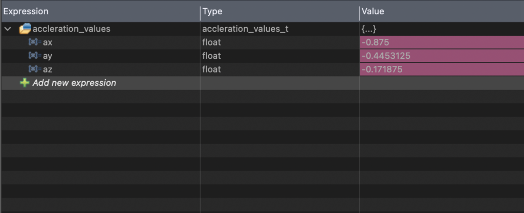
Thats all for the polling mode.
Next, we shall use DMA to start the sending and reception of the data from the sensor.
Stay tuned.
Happy coding 😉
Discussion