Timer synchronization on STM32 allows multiple timers to operate in a coordinated manner using trigger modes, enabling one timer to act as a master and others as slaves. This mechanism supports precise phase alignment, cascaded triggering, and synchronized PWM generation, making it ideal for applications such as motor control, power converters, and multi-channel signal generation where accurate timing relationships are crucial.
In this guide, we shall cover the following:
- Introduction and how does it work.
- Timer internal connection.
- STM32CubeIDE setup.
- Firmware development.
- Results.
1. Introduction and How Does it Work:
Timer synchronization in STM32 microcontrollers is one of the most powerful and underappreciated features of the advanced timer architecture. It allows multiple timers to work together seamlessly, sharing timing information and triggering events in a highly deterministic way. This is achieved through master-slave relationships established via internal trigger connections (known as TRGO and ITR lines), where one timer acts as the master — generating synchronization signals — and one or more other timers operate as slaves, responding to those signals based on configurable trigger modes.
At its core, synchronization ensures that timing operations — such as counting, PWM generation, and capture/compare events — occur in perfect coordination. This is critical in embedded control systems where even microsecond-level misalignment can cause system instability or inefficiency. For example, in three-phase motor control, each PWM signal controlling the motor windings must be precisely phase-shifted relative to the others; even minor timing drift can result in torque ripple or reduced efficiency. Similarly, in DC-DC converters or inverters, synchronized PWM outputs are necessary to control multiple power stages operating in parallel, minimizing noise, improving power balance, and achieving higher overall performance.
The trigger mode plays a central role in synchronization. In this mode, a slave timer listens to an external or internal trigger source — such as an update event or a compare match from the master timer — and reacts by starting, stopping, resetting, or gating its counter based on how it’s configured. This makes it possible to chain timers in complex configurations, such as one timer controlling another to generate time-staggered pulses, periodic ADC conversions, or cascaded event sequences. STM32 timers support multiple synchronization schemes, including reset mode, gated mode, and trigger mode, each providing a different way to control timing relationships between modules.
Another important advantage is hardware-level precision. Unlike software-based synchronization — which depends on CPU timing and can suffer from latency or jitter — hardware timer synchronization operates entirely within the timer subsystem, driven directly by the clock tree and peripheral interconnects. This eliminates software-induced timing uncertainty, making it ideal for high-speed or real-time control applications.
In practical systems, timer synchronization can be extended beyond PWM generation. It can synchronize ADC samplingto ensure data acquisition occurs exactly when PWM outputs reach a certain phase, or align multiple output compare channels for signal generation. Even external triggers (such as encoder pulses or sensor events) can participate in synchronization chains, allowing flexible hybrid designs that blend internal and external timing sources.
Ultimately, timer synchronization provides engineers with a way to build complex, timing-dependent systems that behave deterministically, without relying on processor intervention. This capability allows STM32-based designs to rival or even surpass more expensive real-time hardware in precision and reliability. It’s a cornerstone of any advanced embedded control design — from robotics and motor drives to precision instrumentation and power electronics — where synchronized timing defines the system’s accuracy, stability, and performance.
Timer synchronization in STM32 microcontrollers works by creating a coordinated timing network between two or more hardware timers, where one timer acts as a master and others function as slaves. This coordination is made possible by a series of internal connections called trigger signals (TRGO and ITRx), which allow timers to exchange synchronization events without CPU intervention. The synchronization mechanism ensures that timing operations — such as counting, starting, stopping, or resetting — occur at precisely defined instants relative to each other, enabling highly deterministic system behavior.
When configured in synchronization mode, the master timer generates a trigger output signal (TRGO) based on one of its internal events — typically an update event, a compare match, or an overflow. This TRGO signal is routed internally to other timers via inter-timer trigger inputs (ITR0, ITR1, etc.), which serve as trigger sources for the slave timers. Each slave timer has a trigger selection (TS) field that defines which internal trigger it listens to and a slave mode (SMS) field that determines how it responds when a trigger occurs.
Here’s how it works in practice:
- Master timer event generation: The master timer runs according to its own clock and prescaler settings. When it reaches a predefined condition — such as an update event (counter overflow) — it emits a trigger signal (TRGO).
- Trigger propagation: The trigger is routed internally via the STM32’s timer interconnection matrix to one or more slave timers.
- Slave timer response: The slave timers are configured in one of several slave modes:
- Reset mode: The slave counter resets whenever a trigger is received. Useful for aligning counters.
- Gated mode: The slave counts only while the trigger is active, effectively gating its operation.
- Trigger mode: The slave starts counting on a trigger edge and stops based on its own configuration.
- External clock mode: The slave uses the trigger input as its clock source.
- Synchronized operation: Once synchronized, the timers operate in harmony — their counting, PWM generation, or output compare events remain phase-aligned or sequentially coordinated according to the design.
This synchronization happens entirely in hardware, which is the key to its precision and speed. Unlike software-based coordination, which is subject to interrupt latency and CPU jitter, hardware timer synchronization is driven by the same peripheral bus and clock system, guaranteeing nanosecond-level consistency.
The result is a flexible and scalable timing architecture where multiple timers can be cascaded or aligned to achieve complex time-dependent behaviors. For example:
- PWM synchronization: A master timer generates a trigger that starts multiple slave timers, ensuring all PWM channels begin simultaneously or at controlled phase offsets.
- ADC synchronization: A timer’s TRGO can start ADC conversions at exact intervals synchronized to PWM switching.
- Multi-axis motor control: Three timers can be synchronized with 120° phase shifts to drive a three-phase inverter.
- Event sequencing: One timer can trigger another to create cascaded timing events (e.g., pulse trains or stepper motor control).
In summary, STM32 timer synchronization works by connecting the output of one timer (master) to the trigger input of another (slave) through internal routing lines. By configuring each timer’s trigger selection and response mode, designers can build precise timing networks that operate with deterministic accuracy, low jitter, and zero CPU overhead — a vital requirement in motor control, power electronics, synchronized data acquisition, and other real-time embedded systems.
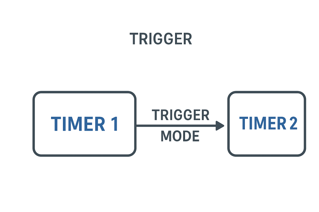
Trigger mode basically controls the start of the slave counter. Here the master timer issues a trigger signal, which resumes the counter on the slave timer.
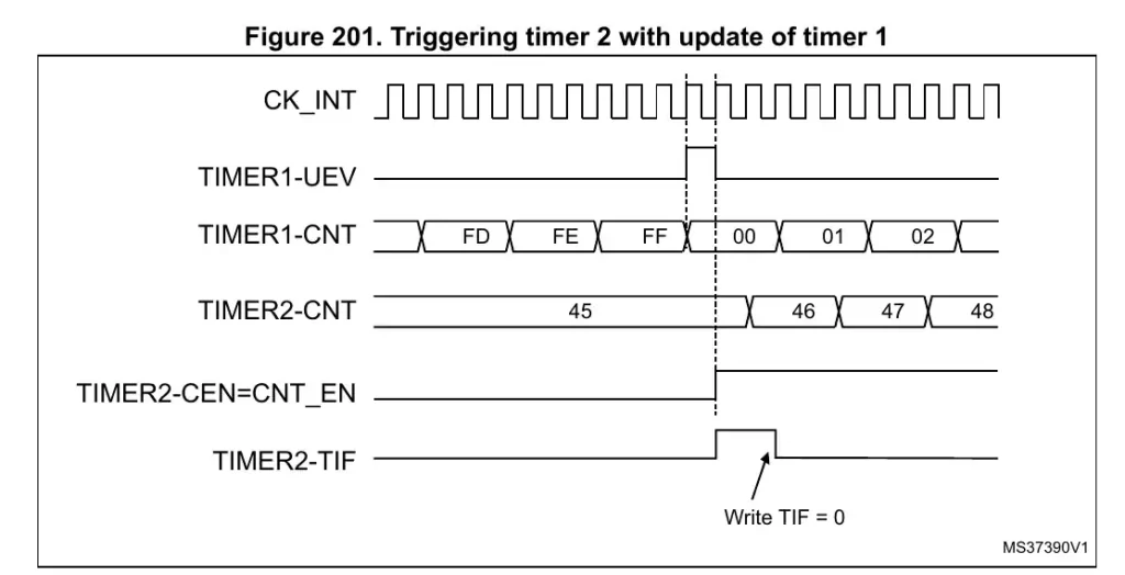
As shown in the picture above, the TIMER 2 (Slave) counter was paused at 45. Once the TIM1 (master) issues Update Event (UEV) signal, the TIM2 counter resumes counting.
Note here that the counter does not reset to 0, rather it just resumes from wherever it was paused. Also the trigger mode only controls the start of the counter, and not the stop.
2. Timer Internal Connection:
As per reference manual of STM32F446RE:
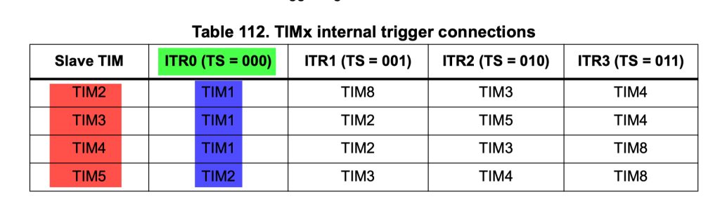
Here the RED box represents the Slave Timers, The BLUE box represents the master Timer, and the GREEN box represents the signal used by the master to control the slave.
So the Timers 2, 3 and 4 can be controlled by the same master, TIM1 by using the signal ITR0.
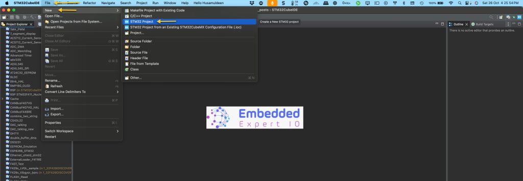
3. STM32CubeIDE Setup:
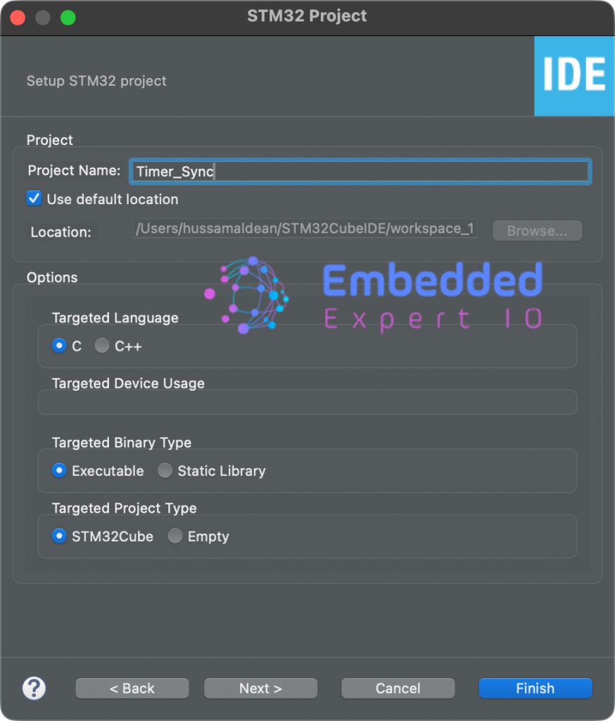
Open STM32CubeIDE after selecting the workspace and create new project as following:
Select the MCU:
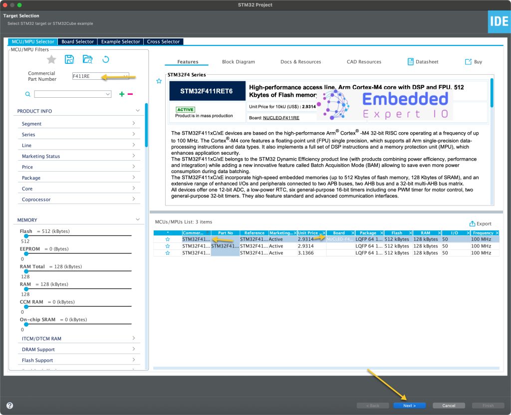
Give the project a name:
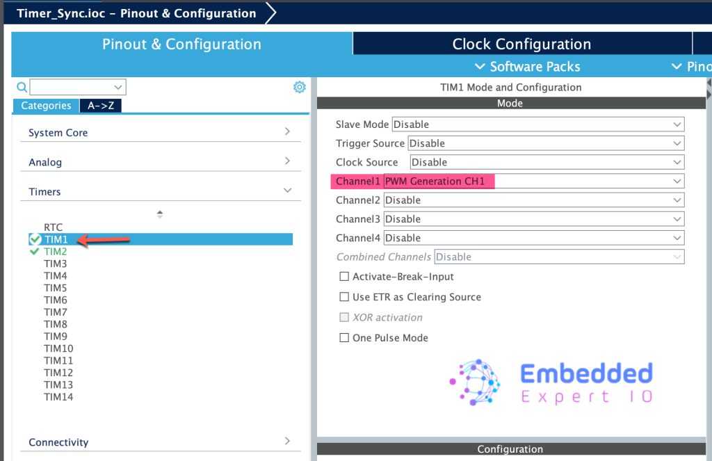
Next, Enable TIM1 since it will be the master as follows:
- Set CH1 as Output PWM
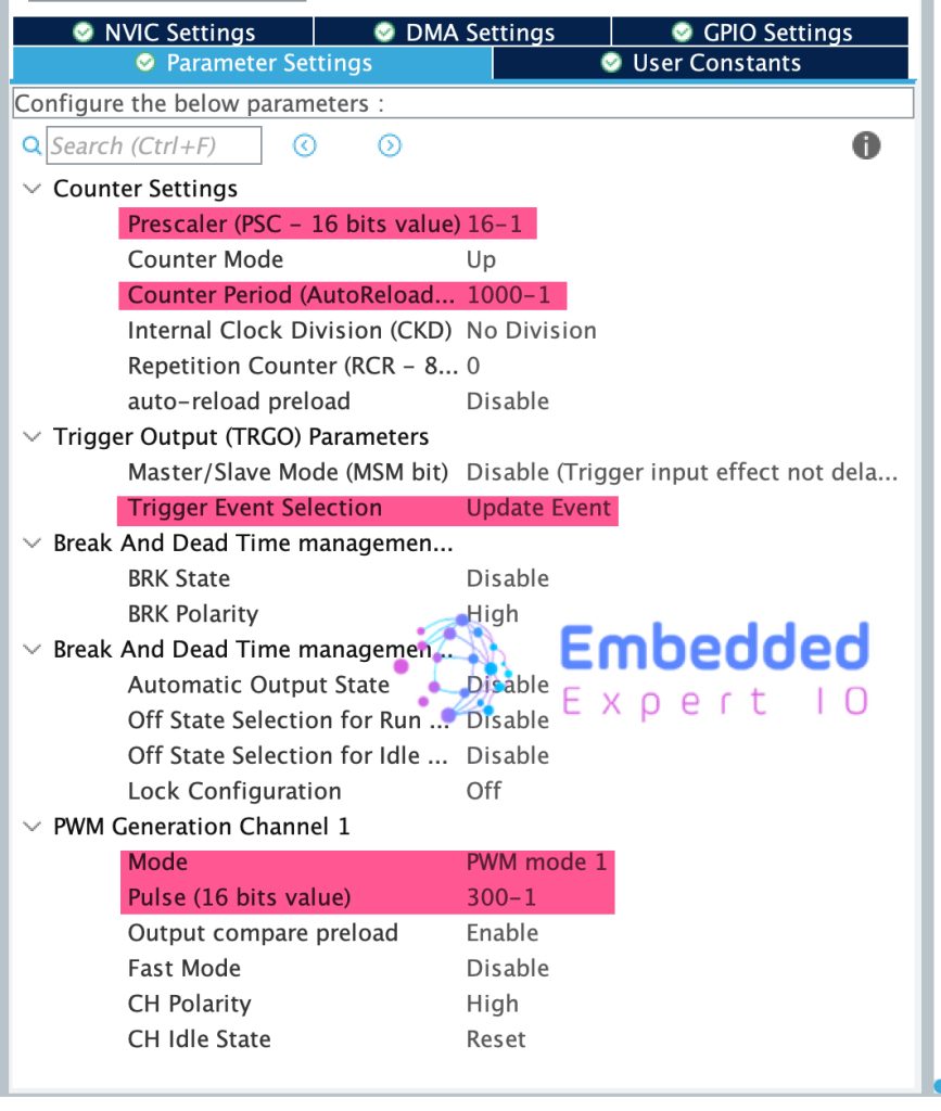
Next, in Parameters Settings set the following:
- Set the PSC to 16-1, this will reduce the timer frequency to 1MHz (default speed is 16MHz for F4).
- Set the Counter Period to 1000-1, this will give PMW frequency of 1KHz.
- Set the trigger event selection to update event.
- Set the pulse to 300-1, this will give 30% duty cycle.
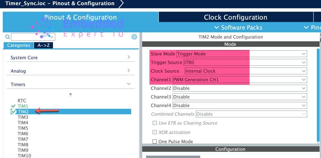
Next, enable TIM2 as follows:
- Slave mode to Trigger Mode.
- Trigger Source to ITR0.
- Clock source to internal.
- Set channel 1 to PWM generation.
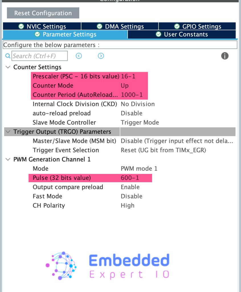
Next, in Parameters Settings:
- Set the PSC and Counter Period to 16-1 and 1000-1 respectively.
- Set the Pulse to 6001, this will give Duty cycle
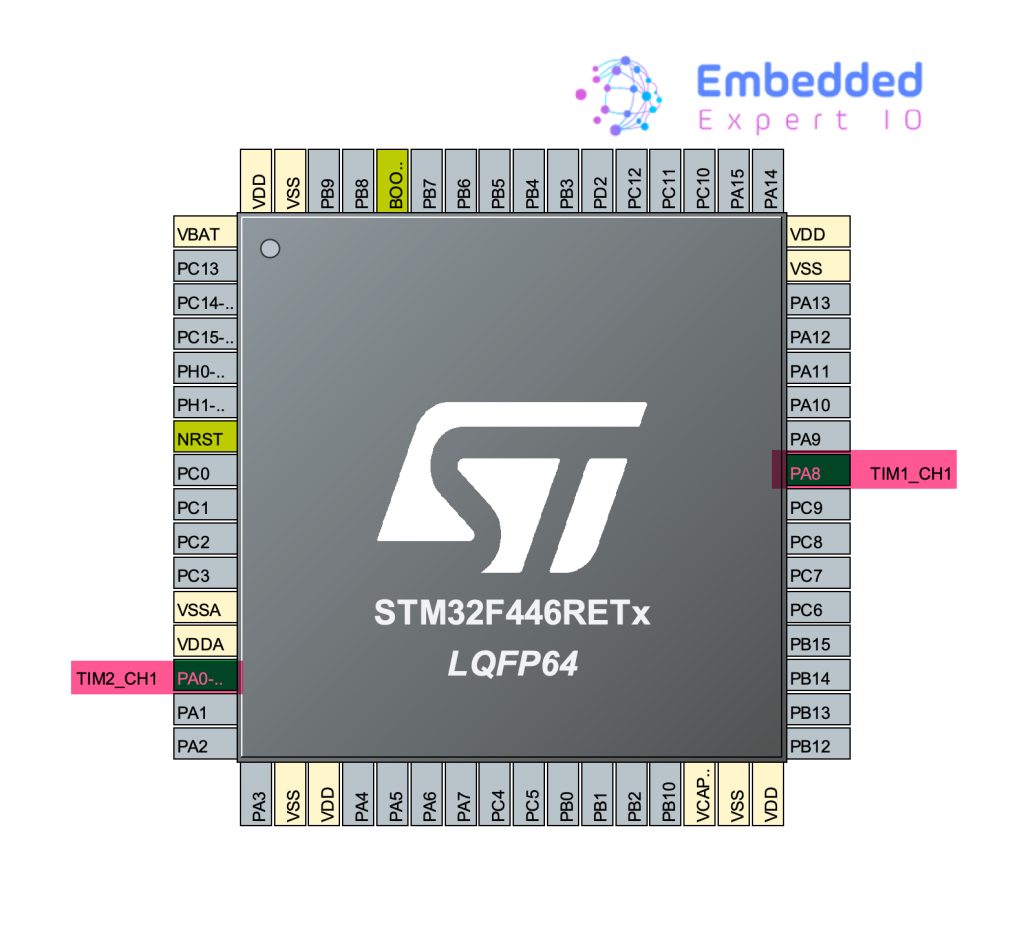
Once the timers have been configured, you will notice that PA0 and PA8 has been enabled for TIM2_CH1 and TIM1_CH1 respectively as follows:
That all for the STM32CubeIDE setup. Save the project and this will generate the code.
4. Firmware Development:
Once the project is generated, main.c will be opened. In main.c file in user code begin 2 in main function, start TIM2 in PWM mode followed by TIM1 in PWM as follows:
  	HAL_TIM_PWM_Start(&htim2, TIM_CHANNEL_1);
  	HAL_Delay(200);
  	HAL_TIM_PWM_Start(&htim1, TIM_CHANNEL_1);
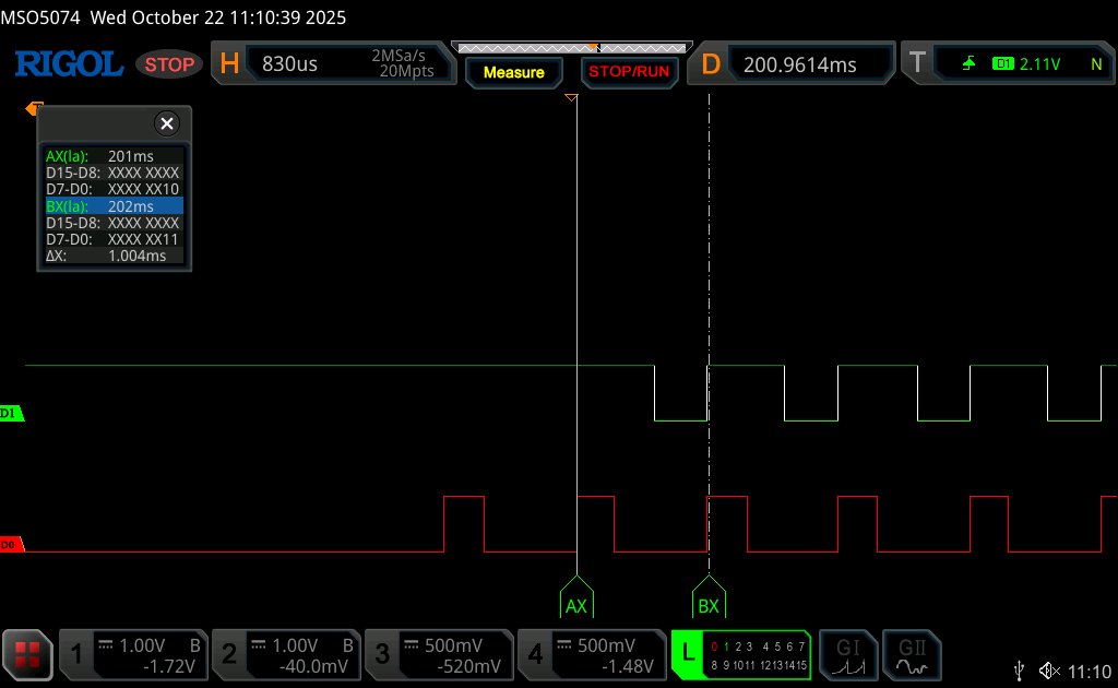
5. Results:
By using oscilloscope or logic analyzer, probe PA0 and PA8.
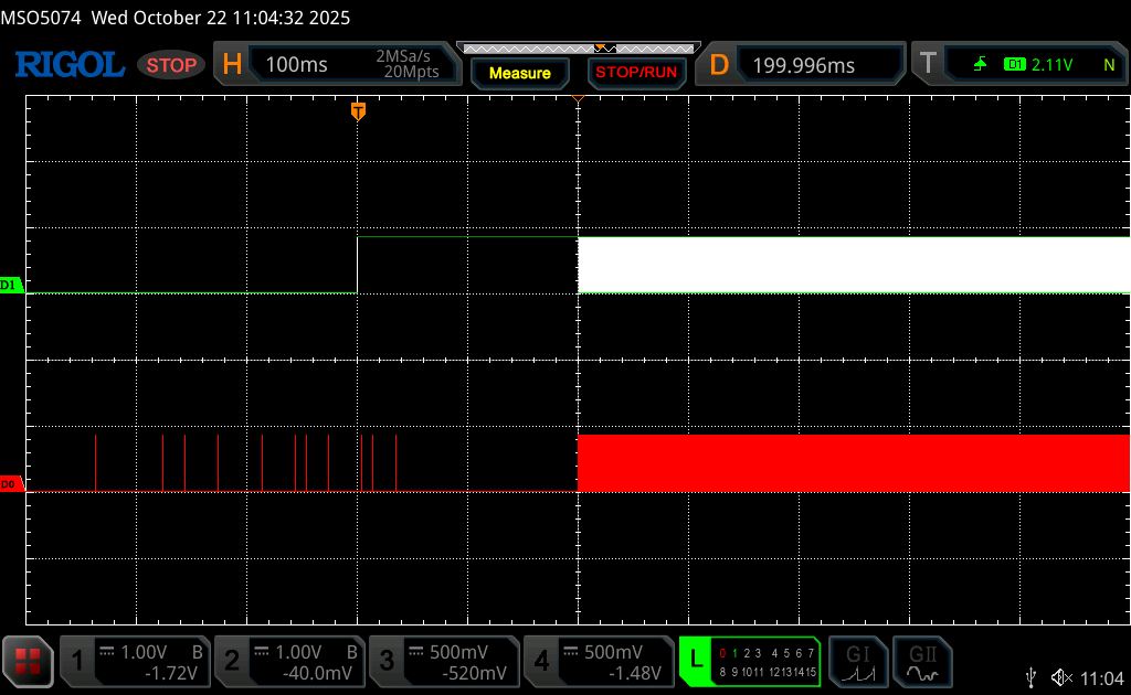
D0 is TIM1_CH1 and D1 is TIM2_CH1.
Note that bit timer started after 200ms from TIM2_CH1 goes to high. Which is expected since there is a delay of 200ms.
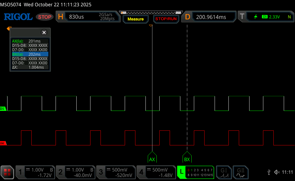
If you zoom in, you find the following:
Notice that TIM2_CH1 started to generate PWM signal after 1ms from TIM1_CH1 started the PWM signal.
We have successfully synchronised two timers.
Notice here with rising edge of each channel, they are aligned together.
Now, you can synchronise TIM3, TIM4 and TIM5 in same manner.
Next, we shall cascade two timers into one timer.
Stay tuned.
Happy coding 😉
Add Comment