The Serial Peripheral Interface (SPI) is one of the most common protocols for connecting microcontrollers to external devices such as sensors, memory chips, and displays, making it an essential tool in any embedded developer’s toolkit. In this guide, we will take a hands-on approach to the SPI peripherals of the STM32F4 family using the Low-Layer (LL) drivers, giving you direct, register-level control over the configuration and data transfer process.
In this guide, we shall cover the following:
- Introduction.
- STM32CubeMX setup.
- Importing the project to STM32CubeIDE.
- Firmware development.
- Results.
1. Introduction:
The Serial Peripheral Interface (SPI) is one of the most common protocols for connecting microcontrollers to external devices such as sensors, memory chips, and displays, making it an essential tool in any embedded developer’s toolkit. Originally introduced by Motorola in the mid-1980s, it has since become a de facto standard supported by virtually every semiconductor manufacturer. If you have ever read data from an accelerometer or flash chip, driven a TFT display, or communicated with an nRF24L01 or LoRa radio module, you have used SPI.
In this guide, we will take a hands-on approach to the SPI peripherals of the STM32F4 family using the Low-Layer (LL) drivers, giving you direct, register-level control over the configuration and data transfer process — while still letting STM32CubeMX generate the initialization code for us.
How SPI works
SPI is a synchronous, full-duplex, master–slave protocol built around four signals:
| Signal | Direction | Purpose |
|---|---|---|
| SCLK | Master → Slave | Serial clock, generated by the master |
| MOSI | Master → Slave | Master Out, Slave In (data to the slave) |
| MISO | Slave → Master | Master In, Slave Out (data from the slave) |
| CS (NSS) | Master → Slave | Chip Select, usually active low |
The master generates the clock and initiates every transfer. Internally, master and slave each hold a shift register, and with every clock pulse one bit is exchanged in both directions simultaneously. This has a practical consequence: every SPI transaction is an exchange, so reading a register from a slave still requires you to transmit (dummy) bytes — that’s what clocks the data back to you.
The Chip Select line selects which slave to talk to. Multiple slaves can share one SCLK/MOSI/MISO bus, each with its own CS line. Although the CS function can be handled in hardware, in practice it is usually a plain GPIO pin — which is why you will typically see it handled alongside the SPI driver, as we do in this guide.
Clocking: CPOL, CPHA, and speed
Two configuration bits — clock polarity (CPOL) and clock phase (CPHA) — define the four standard SPI modes:
| Mode | CPOL | CPHA | Description |
|---|---|---|---|
| 0 | 0 | 0 | Clock idle low, data sampled on rising edge |
| 1 | 0 | 1 | Clock idle low, data sampled on falling edge |
| 2 | 1 | 0 | Clock idle high, data sampled on falling edge |
| 3 | 1 | 1 | Clock idle high, data sampled on rising edge |
The mode and bit order (MSB- or LSB-first) must match what your slave expects — check its datasheet. Most devices use mode 0 or mode 3, MSB first.
SPI owes its speed to its simplicity: no addressing, no acknowledgments, no protocol overhead — just raw clocked bits. On the STM32F4, the clock is derived from the APB bus via a prescaler (fPCLK/2 up to fPCLK/256), reaching 42 Mbit/s on SPI1 and 21 Mbit/s on SPI2/SPI3 of a 168 MHz STM32F407. The trade-off is that correctness is entirely your responsibility: there is no built-in mechanism telling you whether the slave actually received the data.
The STM32F4 SPI peripheral
Depending on the specific device, the STM32F4 family provides up to six SPI peripherals (SPI1–SPI6), spread across the two APB buses — which matters, because the bus clock limits your maximum SPI clock. Each peripheral supports:
- Master and slave operation
- Full-duplex, half-duplex (single bidirectional wire), and simplex (TX-only or RX-only) modes
- 8-bit and 16-bit data frames, MSB- or LSB-first
- All four CPOL/CPHA combinations
- Motorola and TI frame formats
- Baud-rate prescaler from fPCLK/2 to fPCLK/256
- Flexible NSS management: software control, hardware output, or NSS pulse generation between frames
- Hardware CRC calculation and checking with a programmable polynomial
- DMA requests for both transmit and receive
- Interrupts on TXE, RXNE, and error events (overrun, mode fault, CRC error, frame error)
- The BSY flag for detecting the true end of a transfer — critical for knowing when it is safe to release CS, as we will see later
Note that the F4’s SPI has no internal FIFO and only fixed 8- or 16-bit frame sizes — newer families such as the F7, L4, and H7 added both, so keep this in mind when porting code.
Why LL drivers?
ST provides two layers: the HAL, which offers portability and convenience at the cost of significant abstraction, and the LL drivers, which are thin inline functions mapped directly onto the peripheral’s registers. With LL there is no hidden state machine, no runtime overhead, and no surprise behavior — every flag you poll and every bit you set is visible in your code. That makes LL the ideal choice both for performance-critical applications and for anyone who genuinely wants to understand how the peripheral works. Best of all, you don’t have to choose between convenience and control: CubeMX can generate the LL initialization code for you.
2. STM32CubeMX Setup:
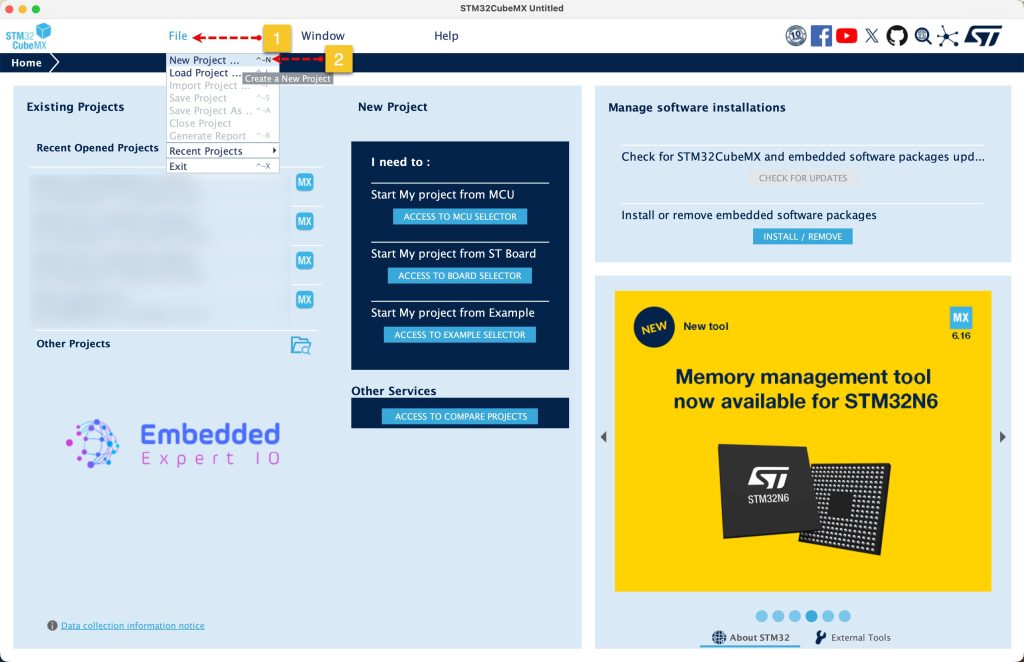
Open STM32CubeMX as start a new project as follows:
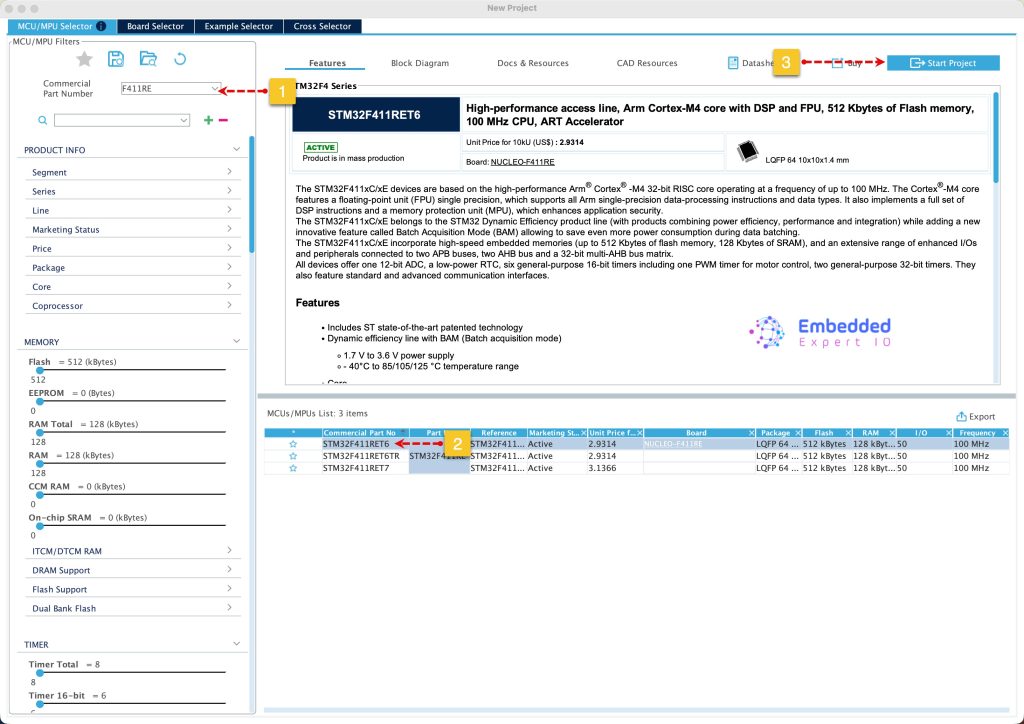
Search for your STM32 MCU, select the MCU and click on Start New Project as follows:
Next, from Connectivity, select SPI1 and enable in Full Duplex Master as follows:
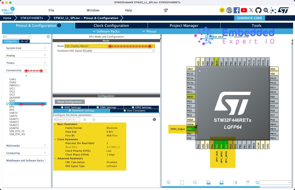
This will set PA5, PA6 and PA7 as SCK, MISO and MOSI respectively.
Next, we need CS pin, we shall use PA0 as CS pin, set PA0 as GPIO Output.
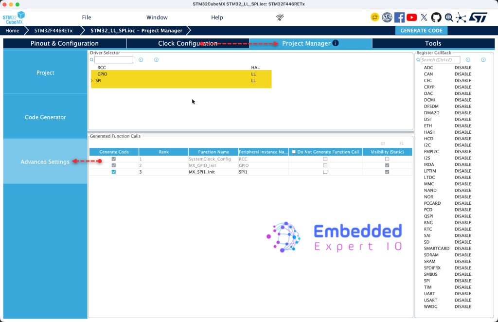
Next, from project manager, Advanced Settings, set both SPI and GPIO as LL as follows:
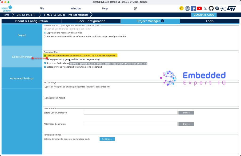
Next, from Code Generator, enable Create peripheral initialization as pair of .c/.h files per peripheral as follows:
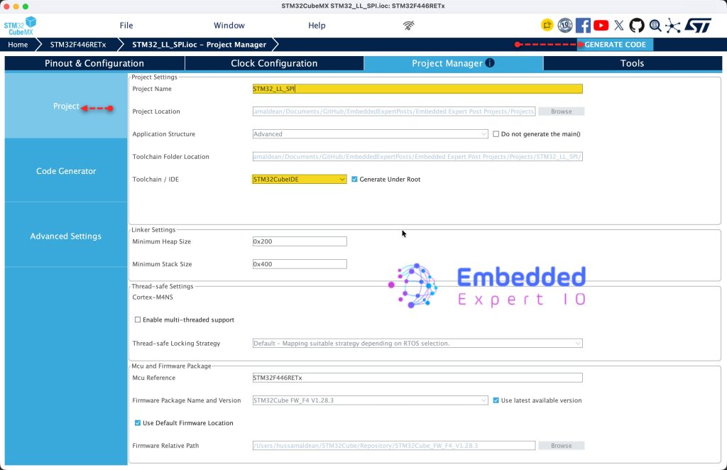
Next, from Project, give the project a name and set toolchain/IDE to STM32CubeIDE and click on Generate Code as follows:
Thats all for the STM32CubeMX setup.
3. Importing the Project to STM32CubeIDE:
Open STM32CubeIDE, select your workspace and click on Launch.
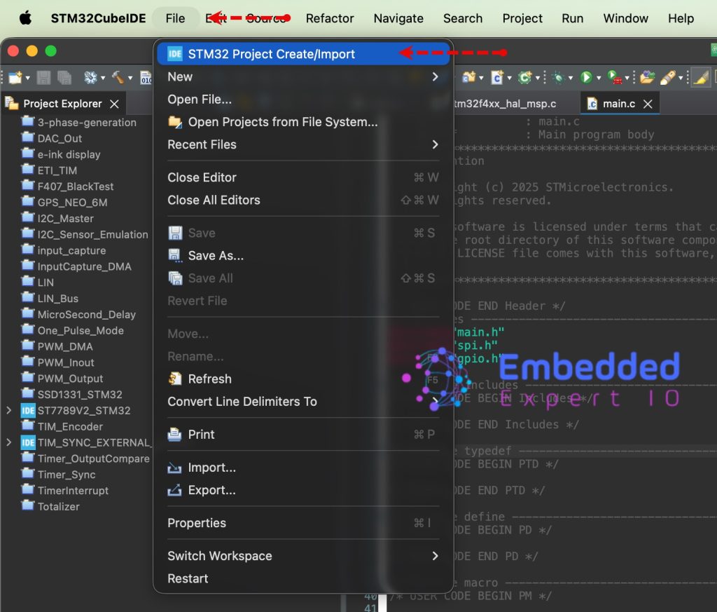
From the IDE, click File and select STM32 Project Create/Import as follows:
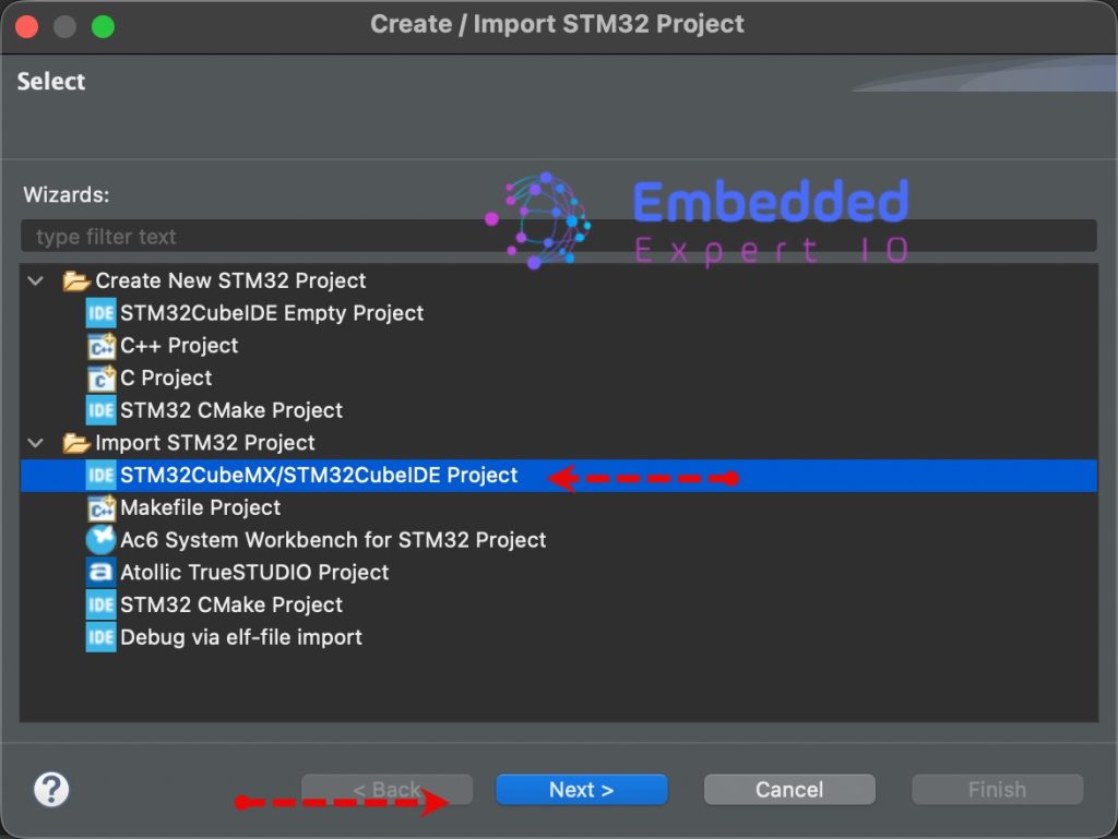
Next, from Import STM32 Project, select STM32CubeMX/STM32CubeIDE Project and click on Next as follows:
Next, select the folder that contains the .ioc file and click on Finish as follows:
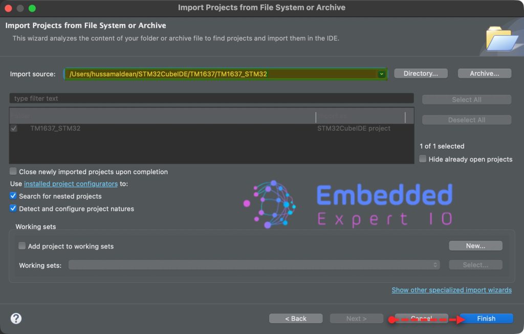
Note: Project name is for reference only.
4. Firmware Development:
Open spi.h header file.
In user begin Prototypes, declare the following function:
void SPI_TransmitBytes(SPI_TypeDef *SPIx, const uint8_t *pData, uint16_t Size);
This function shall transmit N bytes in polling mode and accepts the following parameters:
- SPI instant, which SPI to user such SPI1, SPI2 etc. This guide uses SPI1.
- Pointer to the data to be transmitted.
- Size of the data to be transmitted.
Next, in spi.c source file.
In user code begin 1, declare the following function:
void SPI_TransmitBytes(SPI_TypeDef *SPIx, const uint8_t *pData, uint16_t Size)
Within the function:
First, enable the SPI peripheral if it is not enabled:
LL_SPI_Enable(SPIx);
Next, transmit the data as follows:
- Wait for TX to be empty.
- Send the data.
- Loop for the number of data to be transmitted.
	for (uint16_t i = 0U; i < Size; i++)
	{
	/* Wait until TX buffer is empty */
		while (!LL_SPI_IsActiveFlag_TXE(SPIx))
		{
			;
		}

		LL_SPI_TransmitData8(SPIx, pData[i]);
	}
Finally, wait until the busy flag is cleared:
while (LL_SPI_IsActiveFlag_BSY(SPIx)) {}Hence, the entire function as follows:
void SPI_TransmitBytes(SPI_TypeDef *SPIx, const uint8_t *pData, uint16_t Size)
{

	LL_SPI_Enable(SPIx);

	for (uint16_t i = 0U; i < Size; i++)
	{
	/* Wait until TX buffer is empty */
		while (!LL_SPI_IsActiveFlag_TXE(SPIx))
		{
			;
		}

		LL_SPI_TransmitData8(SPIx, pData[i]);
	}

	/* Wait until the last byte is fully shifted out of the shift register */
	while (LL_SPI_IsActiveFlag_BSY(SPIx)) {}

}
Next, open main.c
In main.c in user code begin PD, declare the following macros:
#define CS_LOW()    LL_GPIO_ResetOutputPin(GPIOA, LL_GPIO_PIN_0)
#define CS_HIGH()   LL_GPIO_SetOutputPin(GPIOA, LL_GPIO_PIN_0)
These micros will handle the CS pin state.
Next, in user code begin PV, declare the following variables:
#define DataSize 5
uint8_t dataBuffer[DataSize];
The databuffer will hold the data to be transferred over SPI with a size determined by DataSize.
Next, in user code begin 2 in main function, we shall fill the array as follows:
for (int i=0;i< DataSize; i++)
{
  dataBuffer[i]=i+1;
}
Finally, in user code begin 3 in while 1 loop:
CS_LOW();
SPI_TransmitBytes(SPI1,dataBuffer,DataSize);
CS_HIGH();
HAL_Delay(1);
- Set the CS pin to low.
- Transmit the data over SPI.
- Set CS pin to high.
- Wait for 1 ms.
Thats all for the firmware.
Save, build and run the project on your board.

5. Results:
By probing PA5, PA7 and PA0 and using either oscilloscope or logic analyzer,. you should get the following:
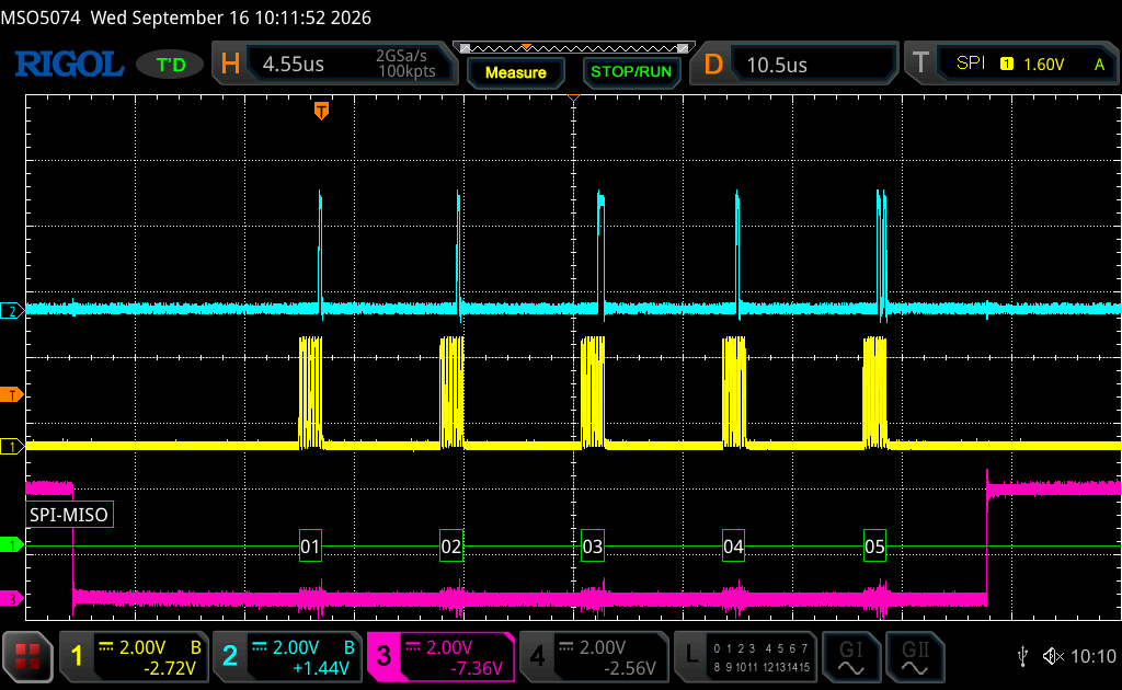
We have successfully transmitted the 5 bytes.
Next, we shall develop a reception code to receive data from a slave device.
Stay tuned.
Happy coding 😉

Add Comment